
Single pass
Topography and resistance, at the same time
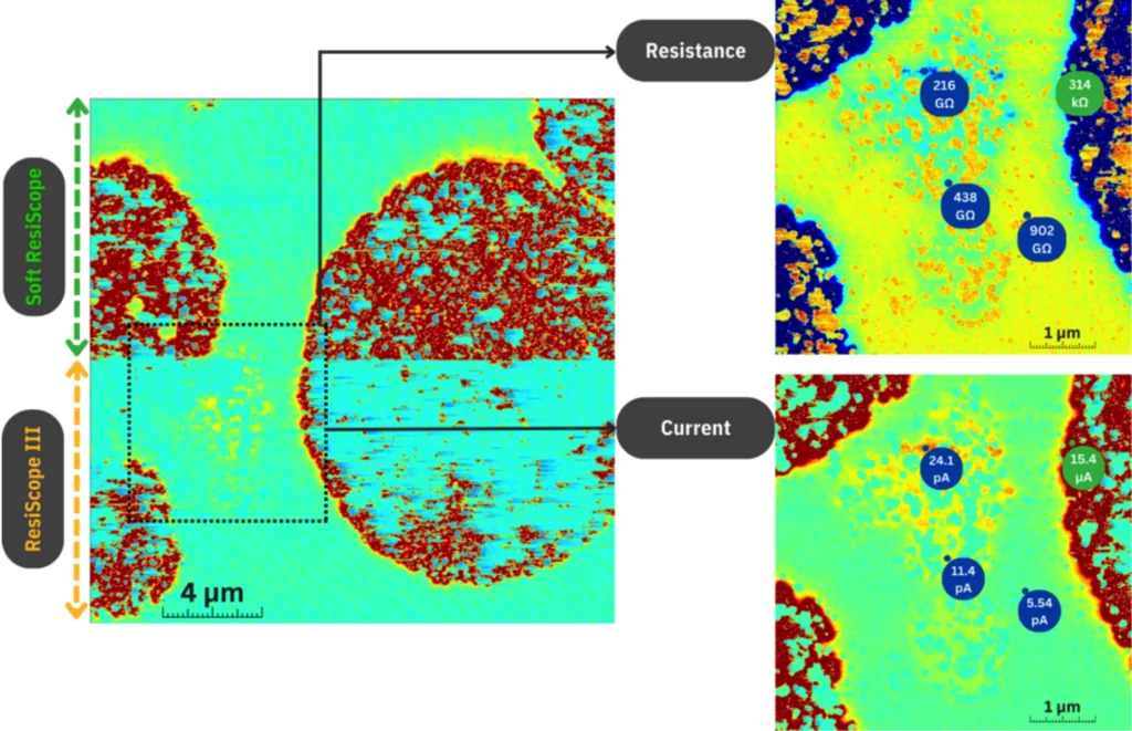
One tip, one trajectory, one pass — both channels come out together.
- 10 orders of magnitude in a single scan
- 10² – 10¹² Ω, no range switching by hand
- Adaptive DSP gain — no saturation, no ghost images
- Resistance and topography acquired together
At a glance
ResiScope™ III in numbers
Adaptive DSP AutoGain re-chooses the gain at every measured point — no manual range switching, no saturation, and real-time current protection for tip and sample.
- Standard C-AFMResiScope™ III
- Current only — resistance inferredDirect quantitative resistance values
- Limited to nA–µA rangefA to µA — 10 full decades
- High force risks sample damageSoft ResiScope™ for fragile samples
- Multiple scans neededResistance + current in one pass
Key Features
ResiScope III
New Capabilities of ResiScope™ III
- Superior accuracy and reduced background noise (Noise floor: < 30 fA RMS)
- Simultaneous PFM + ResiScope measurements
- Full integration with NanoSolution software
- Access to all new future features and updates
- Enhanced compatibility with advanced AFM modes
- Resistance Range: 10² to 10¹² Ω
- Current Range: fA to μA
- Advanced auto-ranging capabilities
- Real-time current protection system
Gallery
Energy
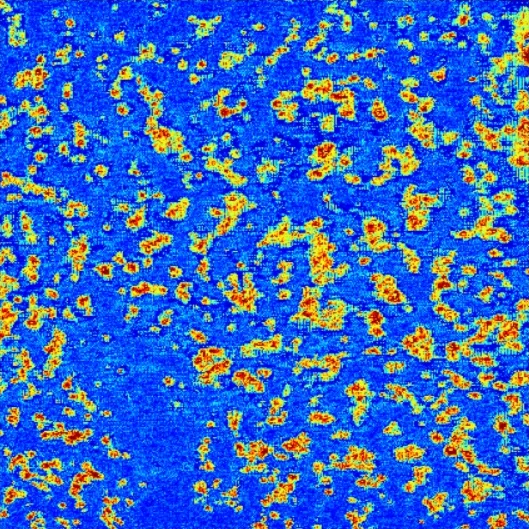
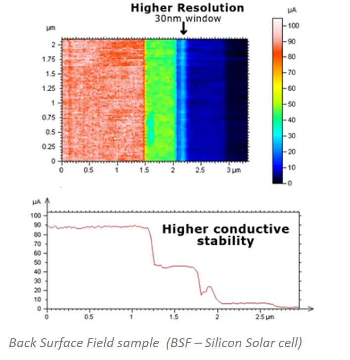
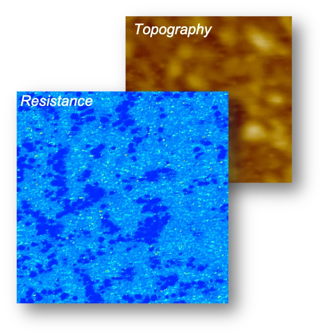
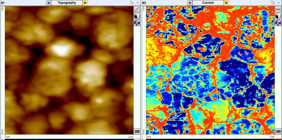
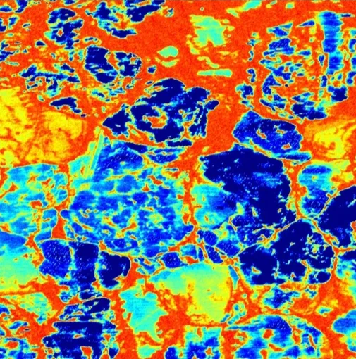
Polymers
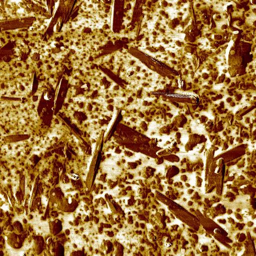
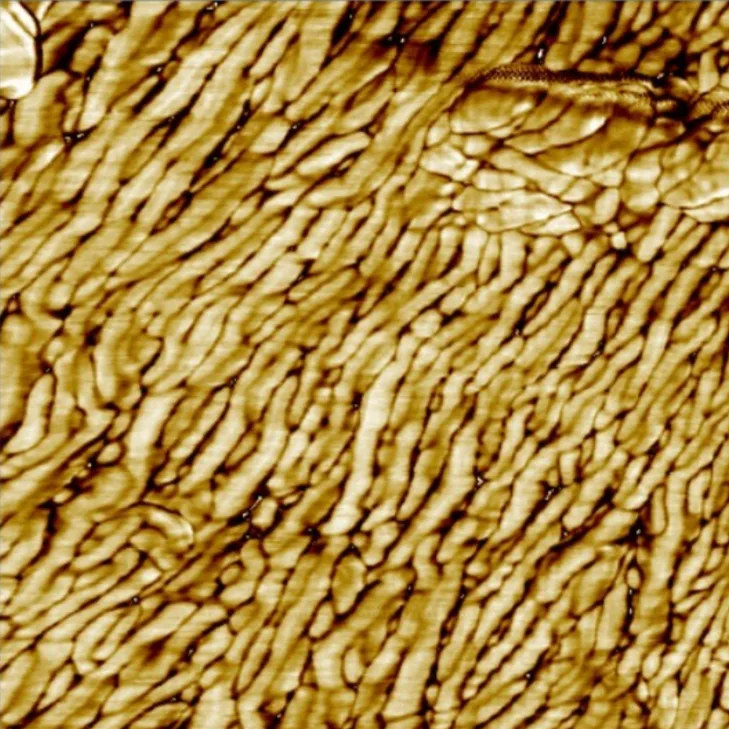
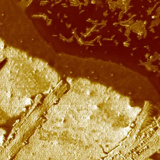
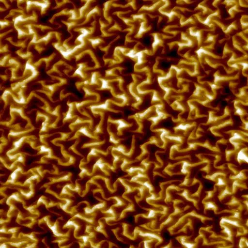
Biological Samples
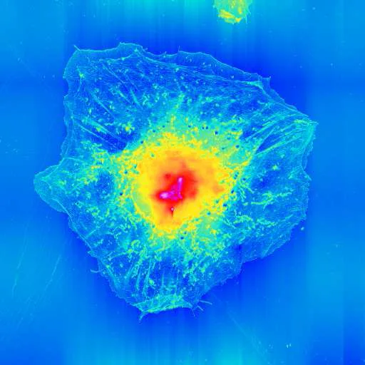
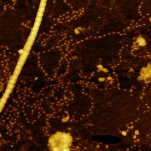
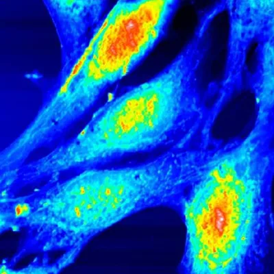
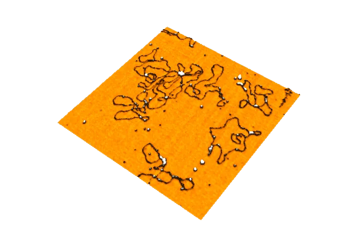
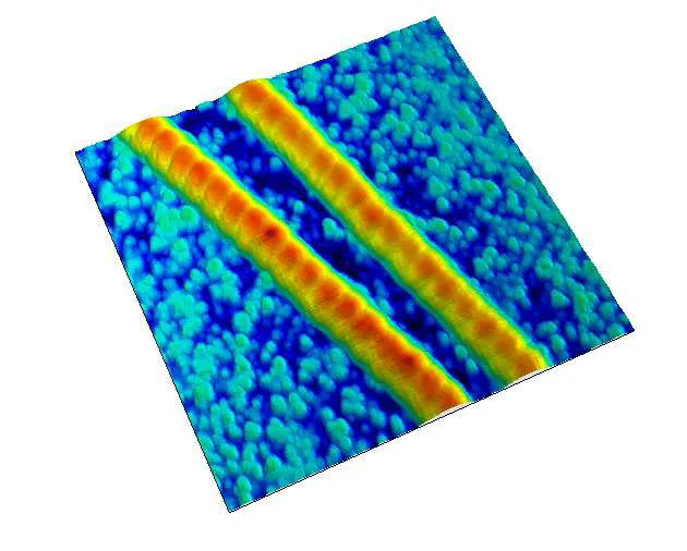
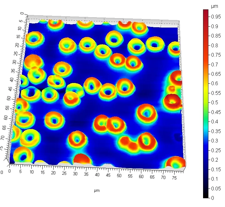
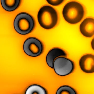
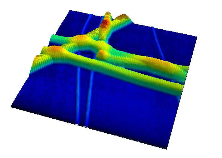
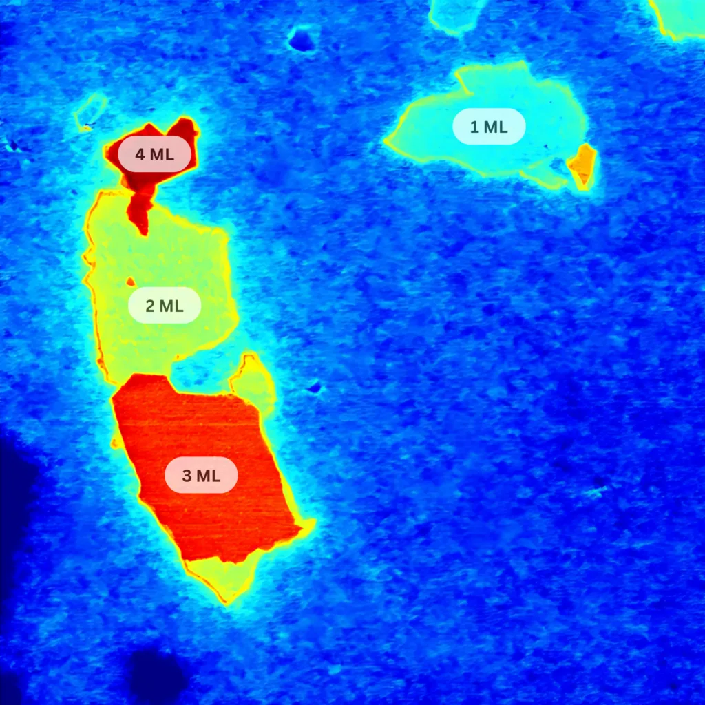
2D Materials
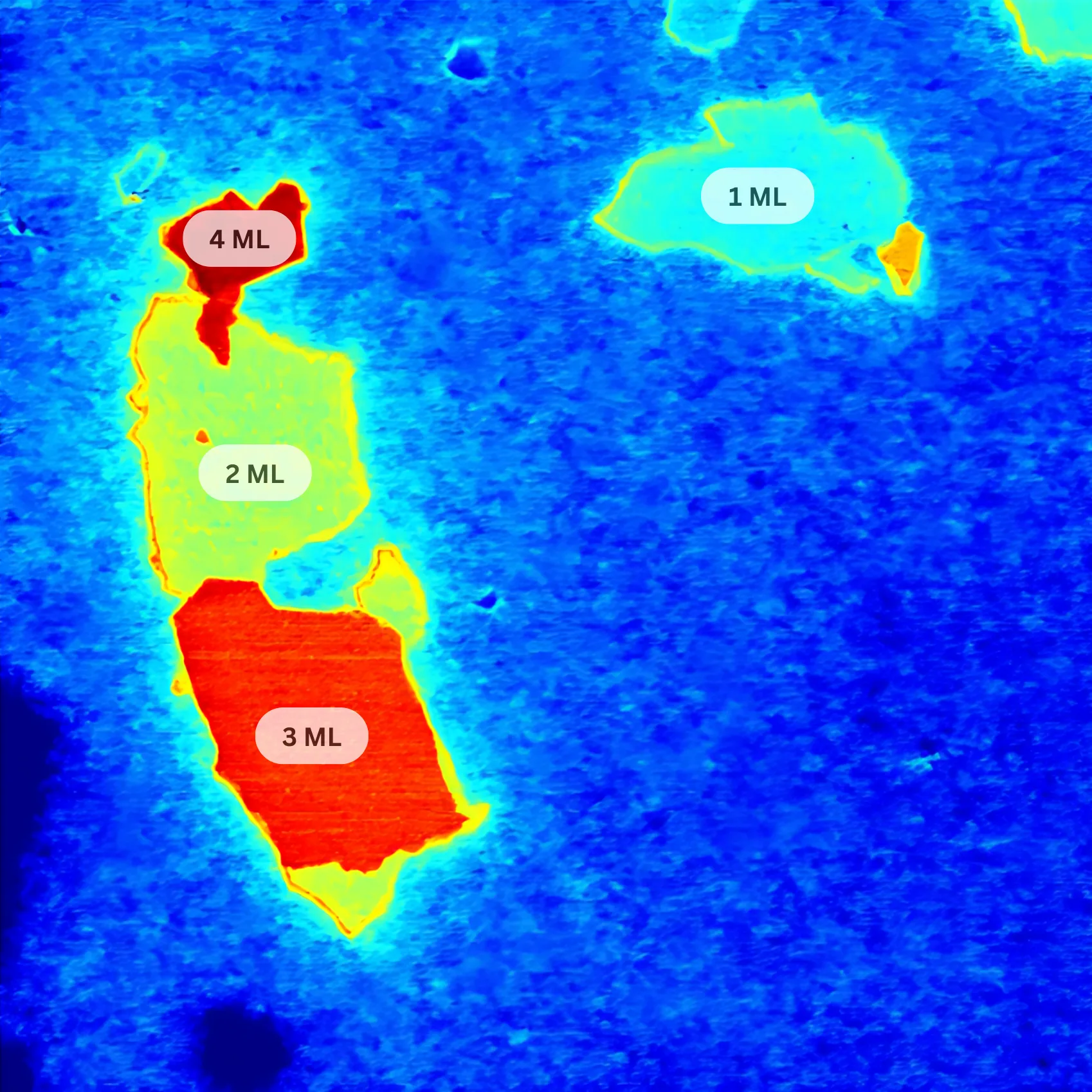
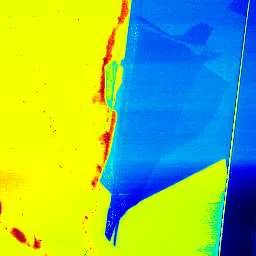
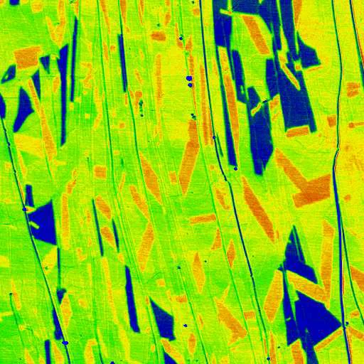
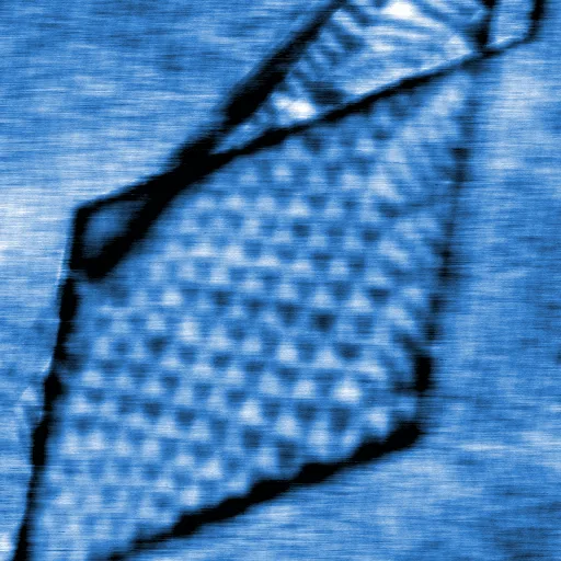
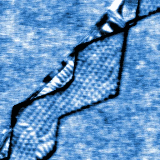
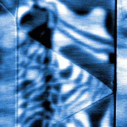
Semiconductors
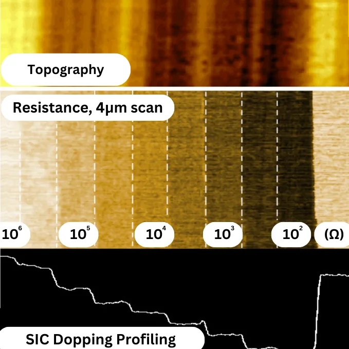
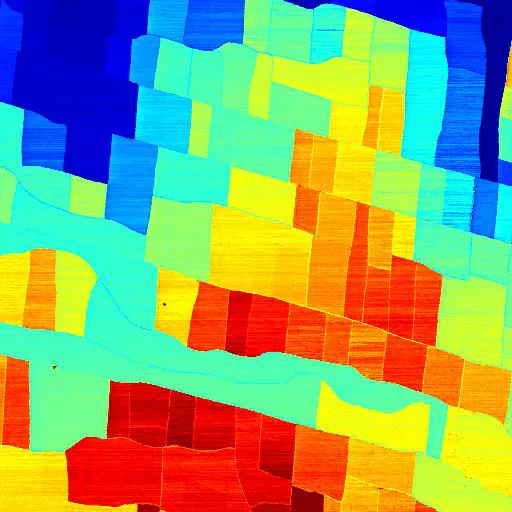
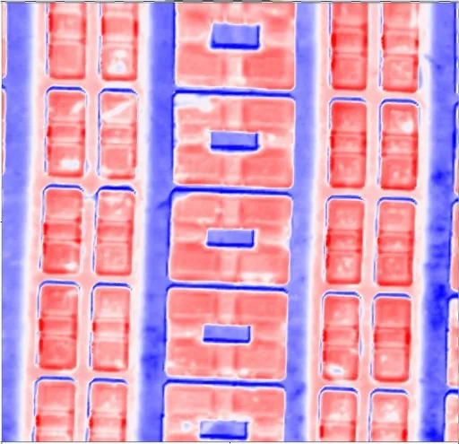
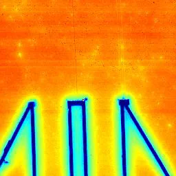
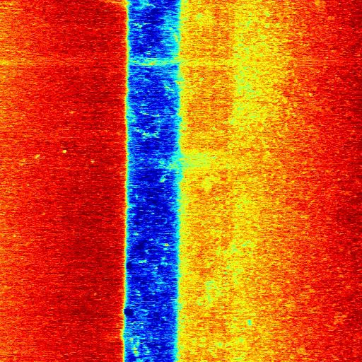
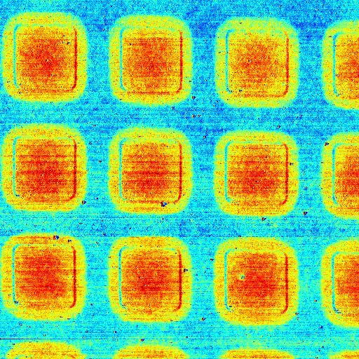
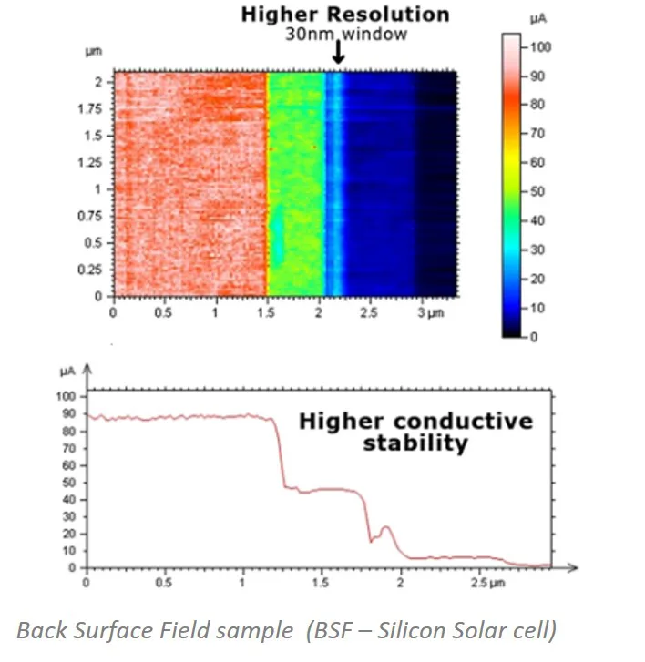
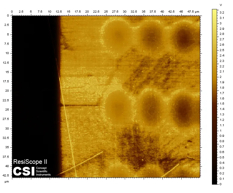
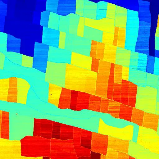
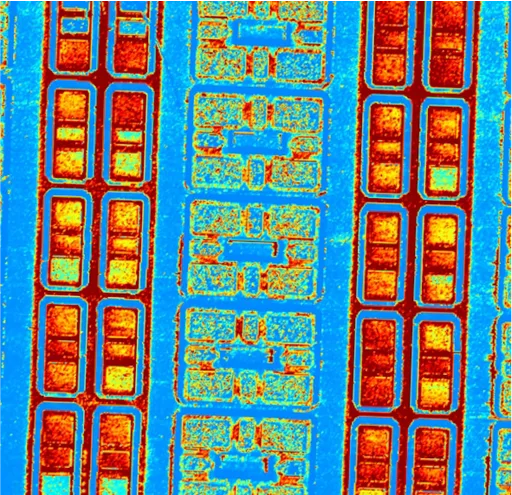
Materials Science
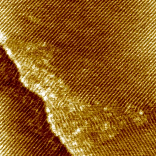
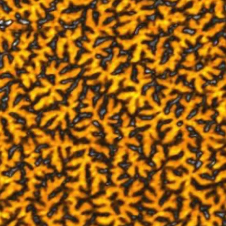
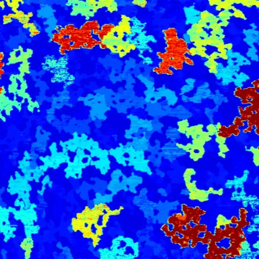
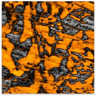
How does ResiScope™ work?
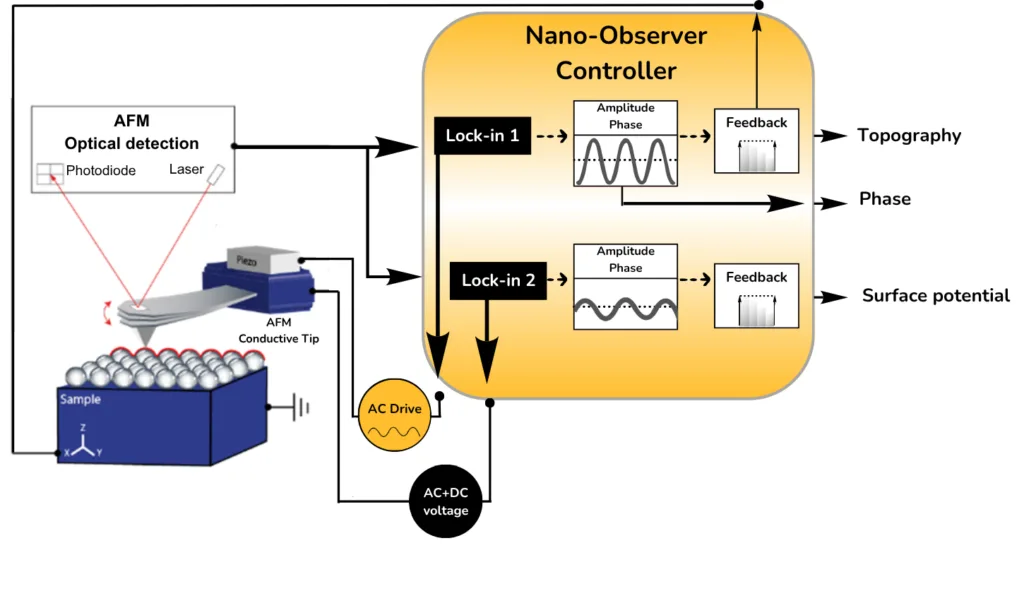
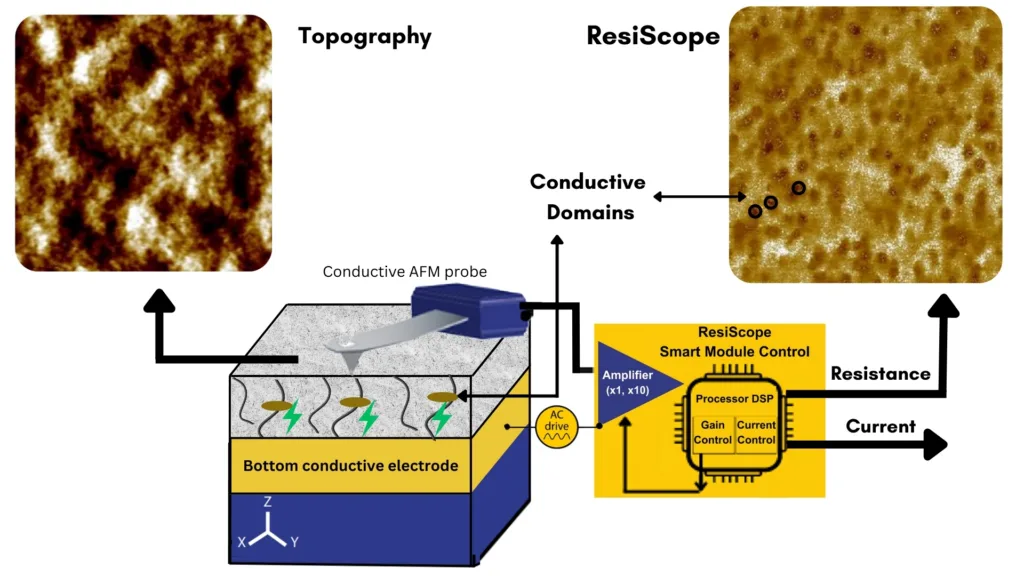
ResiScope™ III is an advanced module for Atomic Force Microscopy (AFM) that enables high-precision electrical measurements at the nanoscale. Here’s an overview of its working principle:
- Conductive Probe:
A conductive AFM tip is used to scan the sample surface.
The tip acts as one electrode, while the sample acts as the other. - Voltage Application:
A DC bias voltage is applied between the tip and the sample. - Current Measurement:
As the tip scans across the surface, it measures the current flowing between the tip and the sample. The current range can be from 100 fA to 1 mA. - Resistance Calculation:
Using the applied voltage and measured current, the system calculates the local resistance. The resistance range covered is from 10² to 10¹² ohms. - Fast Auto-Ranging:
A fast processor-driven auto-ranging system allows for real-time adjustment of the measurement range. This enables accurate measurements across a wide range of conductivities without manual intervention. - Current Limit-Protective Resistance:
Current limitation helps to minimize undesired current-related effects like local oxidation or bimetallic effect. - Simultaneous Resistance/Current/Topography:
While measuring the topography, the system simultaneously captures resistance and current data. This enables comprehensive correlation between physical and electrical properties. - Compatible with All AFM Modes:
ResiScope III is compatible with all AFM modes such as EFM/MFM and standard KFM. Notably compatible with: PFM/ResiScope simultaneously to define real piezo/ferroelectric domains. Contact mode, oscillating modes, and Soft-IC mode for quantitative electrical measurements on soft samples - Data Processing and Visualization:
The collected data is processed in real-time to create high-resolution maps of current and resistance. These maps can be overlaid with topography data for integrated analysis. - Environmental Control:
Measurements can be performed in air, controlled atmospheres, and with temperature control.
Advanced capabilities demonstrated in applications like VO₂ under temperature variation.
The unique design of ResiScope III allows for unprecedented sensitivity and range in electrical measurements, making it a powerful tool for nanoscale electrical characterization across a wide range of materials and applications.
Examples
Organic solar cell layers
Vanadium dioxide (VO₂) thin film
Comparison with Conductive AFM
Case study: polymer battery (80 µm)
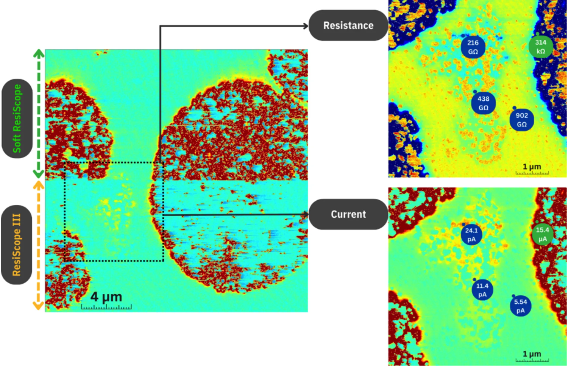
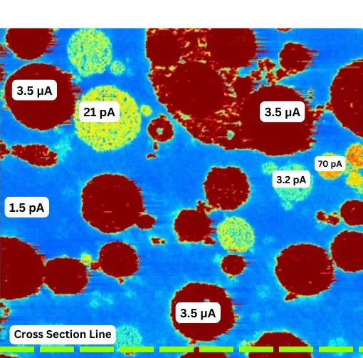
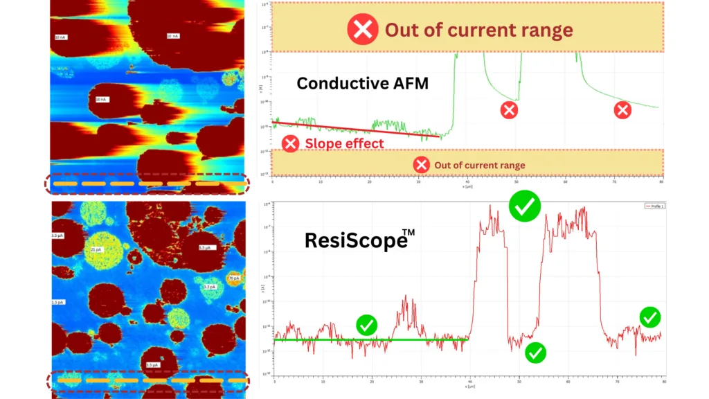
The same area imaged with ResiScope™ and with conventional conductive AFM.
ResiScope Analysis
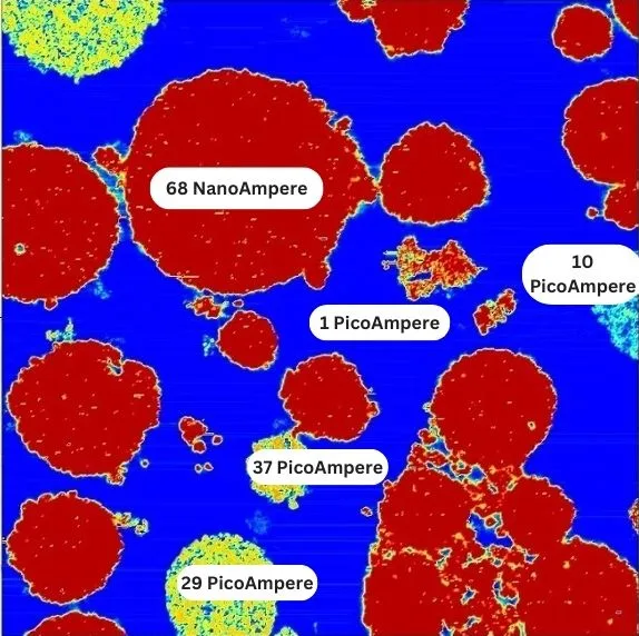
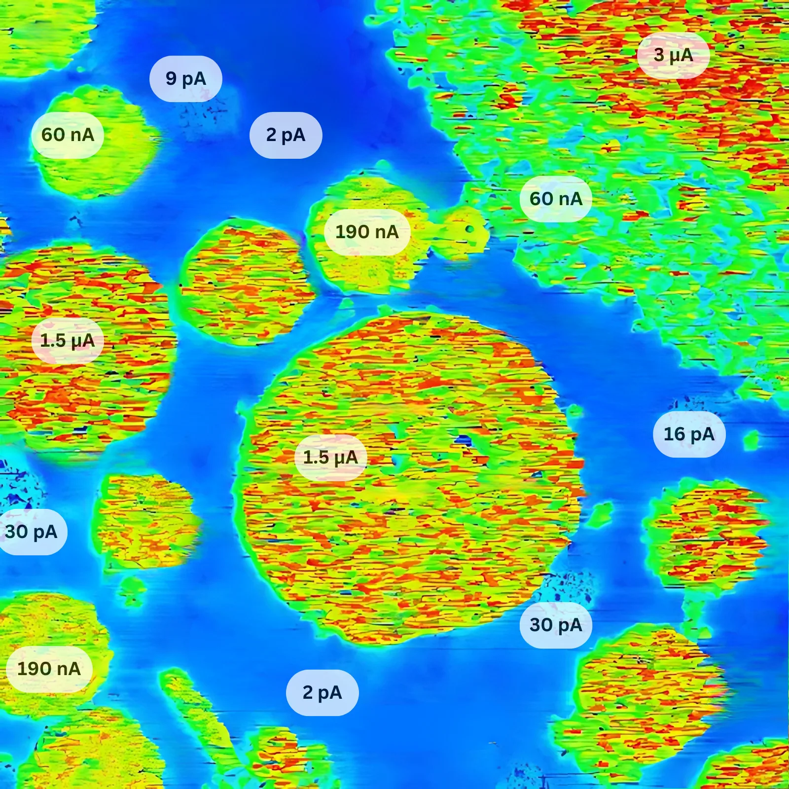
Looking at the ResiScope image (left), we observe distinct domain segregation in the polymer battery sample. The domains exhibit two clear conductivity regimes:
1. High-conductivity domains (red circular regions) displaying current responses in the microampere (µA) range
2. Insulating/low-conductivity domains (blue-orange regions) showing currents in the picoampere (pA) range (1-70 pA)
This clear bimodal distribution indicates well-defined phase separation in the material structure. The high spatial resolution and wide dynamic range, spanning several orders of magnitude in conductivity, enable unambiguous identification of these domains—a crucial factor for understanding the material’s electrical properties and morphology.
C-AFM drawbacks
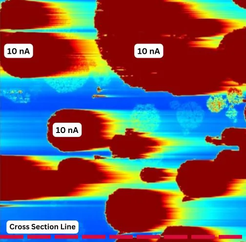
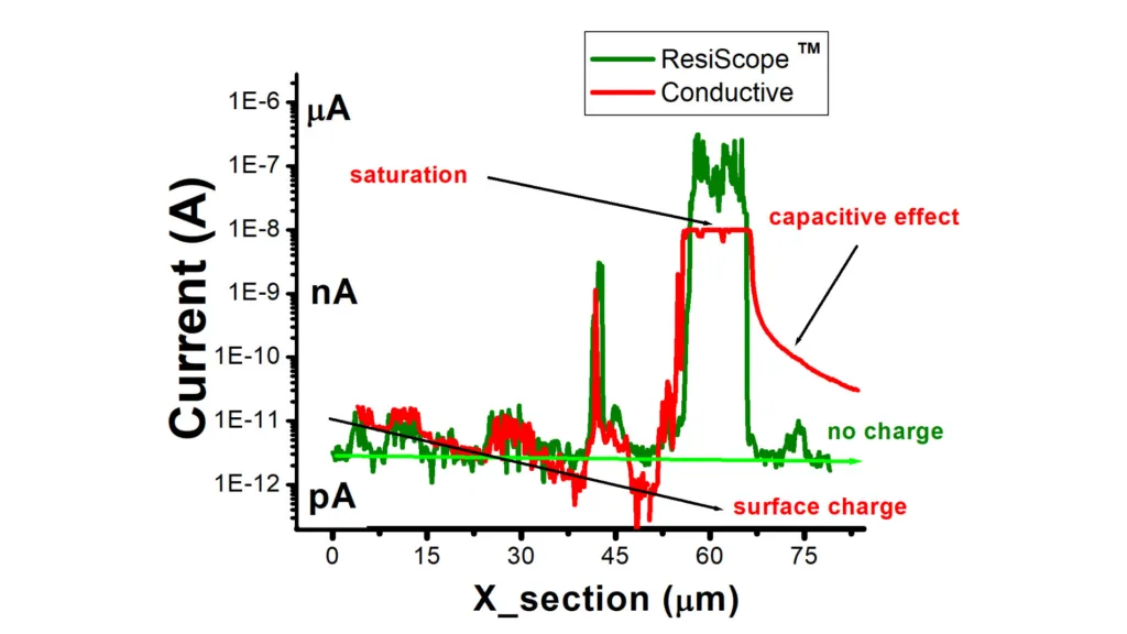
The C-AFM image (right) reveals three distinct types of artifacts stemming from surface charging and capacitive effects, which compromise domain differentiation reliability. Cross-sectional analysis of both images highlights these limitations:
- Current Saturation: The highly conductive domains show saturation at 10 nA (the amplifier’s maximum current), resulting in measured conductivity values approximately two orders of magnitude lower than actual values.
- Capacitive Interference: Capacitive effects prevent accurate measurement of small insulating domains adjacent to highly conductive regions.
- Surface Charging Effects: The absence of protective resistance options in standard C-AFM leads to observable surface charging along the scan direction (left to right), manifesting as a negative tilt in the cross-sectional profile.
ResiScope III vs. C-AFM
- Unrivaled Dynamic Range: ResiScope III offers the highest dynamic range of electrical measurements (50 fA to 1 mA) in a single module, eliminating the need for multiple instruments or sample changes.
- Enhanced Sensitivity: High sensitivity across the entire measurement range with: No capacitive effects No saturation of the preamplifiers Accurate characterization from highly conductive to near-insulating materials
- Advanced Versatility: Full compatibility with all AFM modes (EFM/MFM, KFM) Simultaneous PFM/ResiScope measurements for piezo/ferroelectric domain analysis Advanced oscillating modes and Soft-IC mode capabilities Enhanced temperature control features
- Sample Preservation: Current limiting protective resistance Minimizes local oxidation effects Prevents bimetallic effects Protects delicate or valuable specimens
- Comprehensive Data Collection: Simultaneous mapping of resistance, current, and topography Enhanced correlation between physical and electrical properties Real-time visualization of multiple parameters
- Environmental Adaptability: Operation in air and controlled atmospheres Temperature-controlled measurements Demonstrated capabilities with temperature-sensitive materials (e.g., VO₂)
Specifications
ResiScope III Specifications
- Resistance Measurement Range: 10² to 10¹² ΩCurrent
- Measurement Range: fA to μA
- Voltage Range: ±10 V (adjustable)
- Measurement Speed: Up to 10 kHz (100 μs per measurement)
- Auto-Ranging: Real-time, processor-driven
- Current Control: Active, real-time adjustment
- Noise Level: < 30 fA RMS
- Compatible AFM Modes: Contact Mode Oscillating Mode Force Spectroscopy
- Integration Capabilities: HD-KFM MFM/EFM PFM Environmental Compatibility:Air Controlled Atmospheres Liquids
- Note: Exact specifications may vary depending on the AFM system and environmental conditions. Please consult with a CSInstruments representative for detailed information tailored to your specific application needs.
- Topography Acquisition: Simultaneous with electrical measurements
- Data Output: Real-time resistance and current mapping
- Spatial Resolution: Dependent on AFM tip radius (typically < 10 nm)
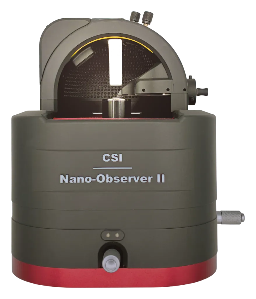
- Software: Integrated with Nano-Observer II control software
- Data Analysis: Built-in analysis tools for electrical property mapping
- Compatible Probes: Wide range of commercially available conductive AFM probes
- Scan area: Up to 100 μm x 100 μm
- Operating Temperature: 10°C to 40°C (standard), extended range available
- Humidity Range: < 80% RH, non-condensing
Application Fields
- Semiconductor Analysis (doping profiling, defect analysis, 2D semiconductors, junction studies)
- Nanoelectronics Research (nanowires, nanotubes, graphene, quantum dots, molecular electronics)
- Material Science (conductive materials, composites, corrosion studies, novel materials)
- Polymer and Composite Studies (conductive polymers, blends, carbon nanotube composites, organic electronics)
- Thin Film Characterization (uniformity analysis, dielectric films, TCO films, solar cell materials)
- Energy Materials (battery electrodes, fuel cells, photovoltaics, thermoelectrics)
- Biomaterials and Bioelectronics (conductive biomaterials, neural interfaces, biosensors)
- Advanced Coatings (anti-static coatings, conductive coatings, smart coatings)
- Memory and Data Storage (RRAM, magnetic media, phase-change memory, spintronics)
- Optoelectronics (photodetectors, LEDs, OLEDs, photovoltaic junctions)
Dynamic range
Conductive AFM vs ResiScope™
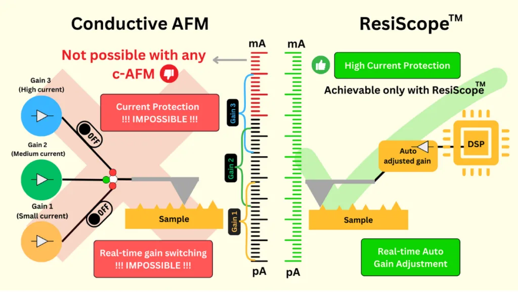
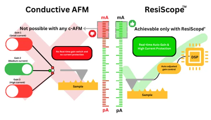
Conductive AFM works with one gain, fixed before the scan: only one window is measured correctly. ResiScope™ re-chooses the gain at every measured point.
- Every decade from pA to µA in one scan
- No saturation above the range, no signal lost in noise below it
- Real-time auto gain and high-current protection for tip and sample
Where it is used
Application fields for ResiScope™ III
Combine and upgrade
Works with — and runs on
Product note
ResiScope™ III product note
Principle, key specifications and application examples in one technical document. We send it to you by e-mail.
FAQ
Frequently Asked Questions
What is ResiScope III?
ResiScope III is a proprietary AFM module developed by CSInstruments for high-precision nanoscale electrical measurements. It simultaneously maps resistance, current, and topography in a single scan, covering a dynamic range of 50 fA to 1 mA in current and 10² to 10¹² ohms in resistance — the widest range available in a single AFM electrical measurement module. It is compatible with the Nano-Observer II AFM and all standard AFM modes.
What is the difference between ResiScope and Conductive AFM (C-AFM)?
The key difference is dynamic range and measurement integrity. Standard C-AFM preamplifiers saturate at fixed current limits (e.g., 10 nA), causing measurement artifacts on samples with mixed conductivity. ResiScope III uses fast processor-driven auto-ranging to cover 50 fA to 1 mA without saturation, capacitive interference, or surface charging artifacts. It also includes a current-limiting protective resistance that prevents local oxidation and sample damage — a critical advantage when measuring delicate materials such as battery electrodes or organic solar cells.
What is the dynamic range of ResiScope III?
ResiScope III covers a current range of 50 fA to 1 mA and a resistance range of 10² to 10¹² ohms in a single module, without changing probes or amplifier settings. This 10-decade dynamic range is achieved through real-time auto-ranging at speeds up to 10 kHz, with a noise floor below 30 fA RMS.
Can ResiScope III be used for battery electrode characterization?
Yes. ResiScope III is particularly well-suited for battery electrode and solid-state battery research. Its wide dynamic range enables simultaneous imaging of highly conductive domains (µA range) and insulating domains (pA range) within the same scan — something standard C-AFM cannot achieve without saturation artifacts. Application examples include polymer battery phase separation mapping, solid-state electrolyte grain boundary analysis, and perovskite solar cell current distribution imaging.
What AFM modes are compatible with ResiScope III?
ResiScope III is compatible with all standard AFM modes, including contact mode, oscillating mode, and force spectroscopy. It can be used simultaneously with PFM (Piezoresponse Force Microscopy) to correlate piezoelectric and electrical properties on the same scan. It also integrates with HD-KFM, MFM, EFM, and environmental control modules including liquid cell and controlled atmosphere.
What materials can be characterized with ResiScope III?
ResiScope III is applicable across a broad range of materials: semiconductors (doping profiling, VO2 phase transitions, SiC staircase resistance mapping); energy materials (battery electrodes, perovskite solar cells, organic photovoltaics); polymers and composites (conductive polymer blends, carbon nanotube composites); 2D materials (graphene, MoS2, nanowires); and advanced coatings and thin films. Its wide dynamic range makes it especially valuable for heterogeneous samples with coexisting conductive and insulating regions.
How does ResiScope III protect sensitive samples during measurement?
ResiScope III includes a current-limiting protective resistance in series with the tip-sample circuit. This actively limits current flow to prevent local oxidation, bimetallic effects, and electromigration damage on sensitive samples. The real-time current control system adjusts automatically, making it safe for use on delicate specimens such as organic semiconductors, biological materials, and thin-film devices.
What is the spatial resolution of ResiScope III?
The spatial resolution of ResiScope III is primarily determined by the AFM tip radius, typically below 10 nm for commercially available conductive probes. Measurements can be performed over scan areas up to 100 µm × 100 µm at speeds up to 10 kHz per measurement point, with simultaneous topography acquisition.
Questions about ResiScope™?
Ask the application scientists behind our AFMs and modes — about your samples, probes, set-up or which mode fits your measurement. We answer every message personally.