

Nanoscale Electrical Characterization of Photovoltaic Materials
Discover how to overcome the limitations of conventional AFM in solar cell research. This application note details how HD-KFM™, ResiScope™, and Soft IC™ modes provide a complete solution for artifact-free conductivity mapping, high-resolution surface potential analysis, and non-destructive characterization.

Unlocking Solid-State Battery Performance with ResiScope™ & HD-KFM™
This note details how to overcome the limitations of conventional AFM for characterizing solid-state polymer batteries. Learn how the synergistic combination of Soft ResiScope™ and HD-KFM™ provides a complete, non-destructive analysis of critical electrical properties.
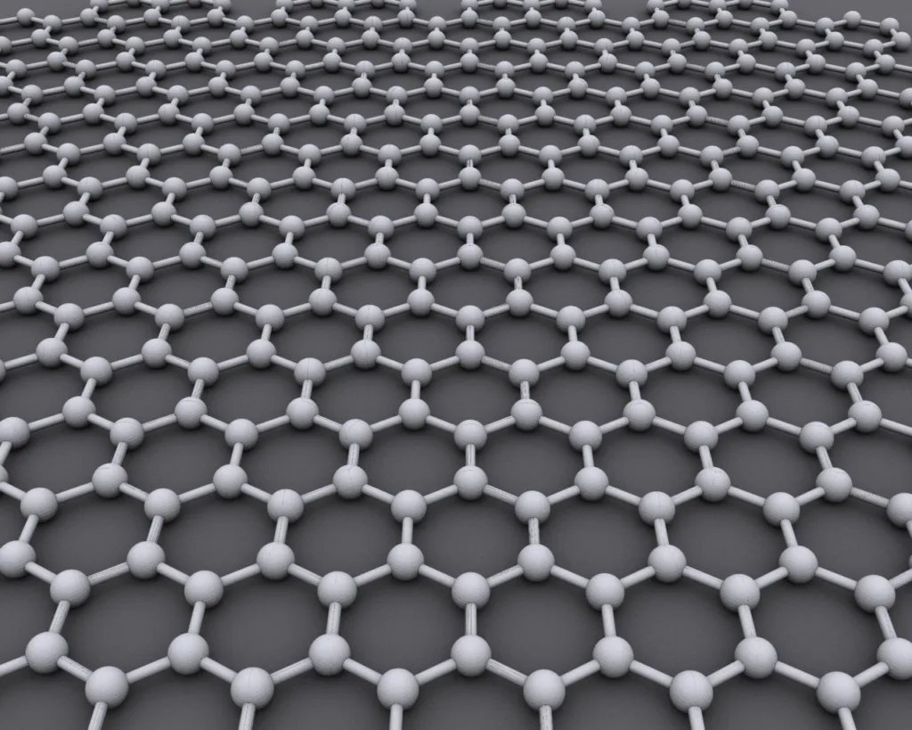
2D Materials: Graphene, hBN & MoS₂
Explore how HD-KFM and ResiScope™ on the Nano-Observer AFM reveal layer-dependent work function, moiré superlattice charge modulation, and conductivity in graphene, hBN, and MoS₂ — from ~100 nm triangular domains to monolayer-by-monolayer electronic structure mapping.
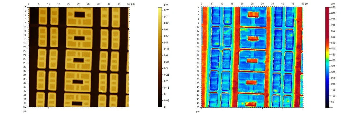
Electrical AFM of Semiconductor Devices
HD-KFM™ and ResiScope™ on the same SRAM area, a silicon dopant staircase from 100 Ω to 1 MΩ, and Soft ResiScope™ on VO₂ during heating.
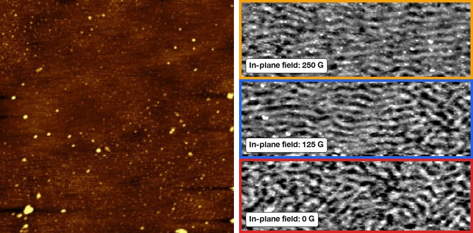
Magnetic Domains Under an Applied Field
MFM with the Variable Magnetic Field Module: domain rotation from 50 to 470 G and field steps within one scan, in plane and out of plane, without sample heating.
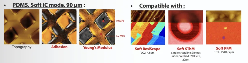
Nanomechanical Mapping of Polymers
Phase imaging, force modulation and Soft MEKA: from morphology to quantitative Young’s modulus and adhesion maps, plus in-situ crystallization.