
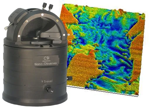
Single pass
Topography and surface potential, at the same time
One tip, one trajectory, one pass — both channels come out together.
- Single pass — no lift, no second line
- 2nd eigenmode harmonic detection
- Tip stays 0.1–0.5 nm from the surface
- Potential contrast at the resolution of the topography
- Sub-surface detection — structures buried under the surface (e.g. nanotubes in a polymer)
Application fields
Key Features
HD-KFM
HD-KFM I represents the next generation of Kelvin Probe Force Microscopy (KFM) technology. This advanced module for the Nano-Observer AFM delivers exceptional sensitivity and resolution in single-pass mode, transforming surface potential measurements at the nanoscale.
Key Features:
- Single-pass operation for faster acquisition and reduced tip wear
- Enhanced sensitivity and resolution compared to standard double-pass methods
- Bimodal dual-frequency design for optimal performance
- High frequency KFM resonance for improved accuracy
- One-click automated measurement system
Comparison:
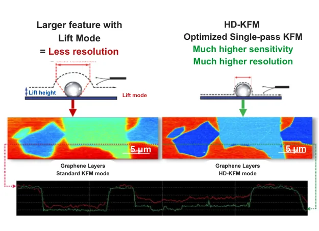
Standard KFM & HD-KFM
Single-Pass Operation
Single-pass operation in HD-KFM represents a significant advancement over traditional Kelvin Probe Force Microscopy techniques:
Elimination of Lift Scans:
- Traditional KFM requires two passes: one for topography and another lifted pass for potential measurement.
- HD-KFM combines both measurements in a single pass, saving time and reducing potential errors.
Proximity to Surface:
- The tip operates at a typical minimum distance of 0.1-0.5 nm from the sample surface.
- This close proximity allows for much stronger interaction with the sample’s electrostatic field.
- Compared to standard KFM (10-100 nm lift height), HD-KFM probes an electrostatic field 100-10,000 times stronger.
Enhanced Resolution and Sensitivity:
- Closer proximity leads to significant improvements in lateral resolution.
- Sensitivity is greatly enhanced, allowing for detection of subtle variations in surface potential.
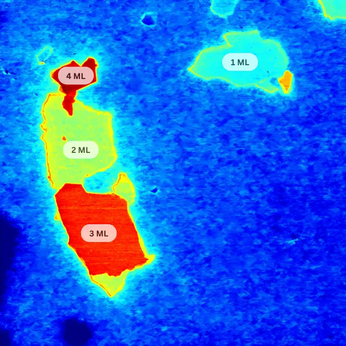
- Enables clear differentiation between features like single and multiple layers of 2D materials.
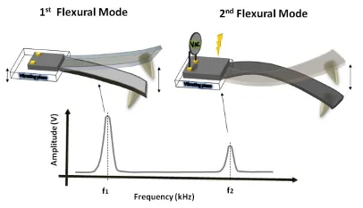
Bimodal Dual Frequency Excitation
Topography Frequency:
- The first flexural mode of the cantilever is excited mechanically.
- This frequency is used to measure and control the sample topography.
- Allows for precise tracking of surface features without interference
Surface Potential Frequency:
- The second flexural mode of the cantilever is excited electrically.
- This separate frequency is dedicated to measuring surface potential.
- Enables simultaneous, independent measurement of topography and surface
Signal Amplification:
- The use of the second eigenmode for electrical excitation inherently amplifies the signal.
- This amplification occurs even with very small applied AC voltages.
- Results in improved signal-to-noise ratio and higher sensitivity to small potential differences.
Enhanced Signal Amplification:
- The VAC bias is fine-tuned to the second eigenmode of the cantilever.
- This tuning amplifies the signal by the Q factor of the second mode.
- The Q factor amplification can be significant, often 100 times or more, greatly enhancing sensitivity.
Improved Stability:
- The second eigenmode has a stiffer effective spring constant compared to the fundamental mode.
- This increased stiffness provides more stable oscillation during surface scanning.
- Stability translates to more reliable and consistent measurements, especially on challenging samples.
Automated Frequency Optimization:
- The Vac bias is fine-tuned to the Second eigenmode automatically by the software without user intervention.
- Patented algorithm selects the best frequency position around the resonance peak.
- Achieves better resolution and sensitivity through optimized frequency selection.
Specifications
Technical Parameters:
- Potential Resolution: < 5mV
- Spatial Resolution: Down to 10nm
- Scan Speed: Up to 2 lines/s in single-pass mode
- Operating Frequencies: First mode: 50-500 kHz Second mode: 200-1500 kHz
- Compatible Tips: Metal-coated and highly doped silicon probes
System Requirements:
- Compatible with Nano-Observer AFM systems
- Digital controller with high-speed data processing
- Automated frequency detection and tracking
- Built-in calibration protocols
Application Fields
- Materials Science (Surface potential mapping, work function measurements, defect detection, thin film analysis)
- Semiconductors (Doping profiling, device characterization, failure analysis, nanoscale electronics)
- 2D Materials (Layer identification, electronic property mapping, substrate interaction studies, defect analysis)
- Polymers (Charge distribution mapping, blend differentiation, aging studies, nanoscale polymer electronics)
- Life Sciences (Biomaterial characterization, cell membrane charge mapping, protein/DNA charge analysis, bioelectronics)
Examples
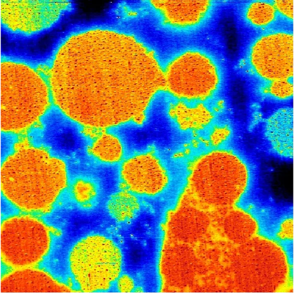
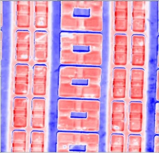
Next generation
Need more? HD-KFM™ III
Discover HD-KFM III with enhanced features like better accuracy and lower background noise, simultaneous MFM+HD-KFM measurements, dC/dZ capabilities for dielectric measurements, and MFM with EFC (Electrical Field Compensation) option.
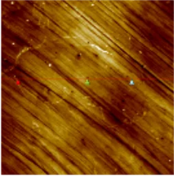
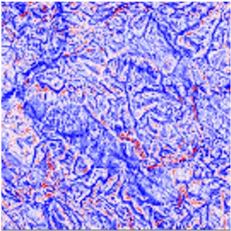
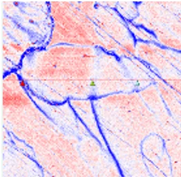
Example: simultaneous measurements of surface potential, topography and magnetic domains on a polished alloy sample
Application note
HD-KFM™ in battery research
How single-pass HD-KFM maps the surface potential of battery materials, with the measurement set-up and results.
Product note
HD-KFM™ I product note
Principle, key specifications and application examples in one technical document. We send it to you by e-mail.
Questions about HD-KFM™?
Ask the application scientists behind our AFMs and modes — about your samples, probes, set-up or which mode fits your measurement. We answer every message personally.