
Key takeaways
- HD-KFM™ III, single-pass KPFM on the Nano-Observer II, resolves grain-boundary potential contrast in perovskite thin films at sub-10 nm resolution.
- Illuminated KPFM (surface photovoltage) compares dark and illuminated conditions on the same area.
- ResiScope™ III maps grain-level conductivity in perovskite films and doped-layer interfaces in silicon solar cells, over several orders of magnitude in one pass.
- Soft ResiScope™ separates conductive P3HT and insulating PMMA domains in organic solar-cell blends without damaging the film.
Animated story
The same question, at the nanoscale
What a solar cell does under light depends on how the light arrives. Reproduce the angle, and you reproduce the condition — then measure the response where it happens, on the surface.
01
The same range the sun covers over a day
Irradiance follows the elevation, from 20° to 90°.
02
Reproduce the angle
…and you reproduce the condition the cell sees in the field.
03
The same sweep, on the microscope
Continuously adjustable on a graduated arc, locked at any angle onto the sample.
Why Macroscopic Measurements Are Not Enough
Perovskite solar cell efficiency is governed by nanoscale phenomena that bulk measurements cannot resolve: grain boundary recombination, local ion migration, and interfacial charge trapping occur at length scales of 5–500 nm — precisely the domain of AFM-based electrical characterization.
Despite impressive certified efficiencies above 26%, perovskite devices suffer from spatial heterogeneity at the grain level. Two grains separated by 10 nm can differ by 100–300 mV in surface potential, act as current-blocking barriers, or provide preferential ion migration pathways. These variations determine whether grain boundaries are benign, beneficial, or detrimental to device performance.
Techniques like EQE, J-V characterization, and impedance spectroscopy yield area-averaged responses. They cannot localize the source of Voc loss, FF degradation, or hysteresis. KPFM and conductive AFM provide the missing spatial dimension, mapping potential and current distributions with sub-10 nm resolution across the exact grain structures responsible.
Surface Potential Mapping of Grain Boundaries
Kelvin Probe Force Microscopy (KPFM) measures the contact potential difference (VCPD) between a conductive AFM tip and the sample surface at each pixel, producing a quantitative map of local work function and surface potential. In perovskite films, this directly reveals the electrostatic landscape governing charge separation and transport.
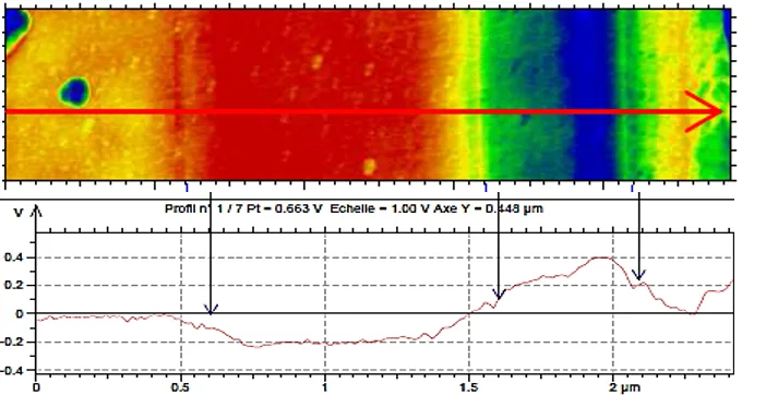
Figure 1. Surface potential map of a perovskite thin film. HD-KFM III single-pass measurement on the Nano-Observer II resolves grain boundary potential contrast at sub-10 nm resolution. Bright regions (higher potential) at grain boundaries indicate local work function variations of 50–200 mV, consistent with defect-induced band bending and ion accumulation at grain interfaces.
CSInstruments’ HD-KFM III operates in true single-pass mode with bimodal dual-frequency excitation at an effective tip-sample distance of 0.1–0.5 nm — dramatically shorter than conventional lift-mode KFM (20–100 nm). This proximity delivers 100–10,000× greater electrostatic sensitivity and sub-10 nm spatial resolution, enabling visualization of individual grain boundary widths and intragranular potential gradients that lift-mode KPFM cannot resolve.
Grain Boundary Potential
Identify whether grain boundaries act as charge recombination centers (negative potential barriers) or charge transport highways (positive potential accumulation).
Built-in Electric Field
Map the built-in potential across ETL/perovskite and HTL/perovskite interfaces. Direct measurement of local band bending under dark and illuminated conditions.
Illuminated KPFM
Surface photovoltage mapping under controlled illumination reveals photogenerated carrier separation, local Voc variations, and charge recombination hotspots.
Ion Migration Tracking
Time-resolved KPFM captures ion redistribution under applied bias, correlating surface potential drift with J-V hysteresis behavior.
Resistance Mapping of Photovoltaic Films
Conductive AFM techniques reveal the current and resistance distribution across the photoactive layer — information critical for understanding shunting, current collection uniformity, and layer-to-layer charge transport. The challenge in photovoltaic samples is the enormous dynamic range: conductive grain cores and resistive grain boundaries or interfacial layers may differ by 4–8 orders of magnitude in resistance within a single scan area.
Standard C-AFM amplifiers saturate when encountering this range, forcing researchers to choose between resolving high-resistance or low-resistance regions — never both simultaneously. ResiScope™ III solves this with real-time DSP-driven AutoGain, covering 10² to 10¹² ohms (fA to μA) in a single continuous scan with no manual adjustment.
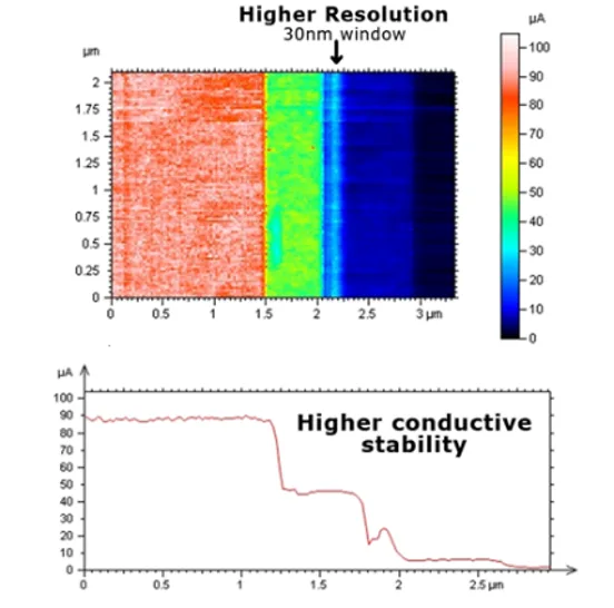
Figure 2. Silicon solar cell resistance mapping. High-resolution ResiScope™ scan resolving doped layer interfaces and resistance gradients across multiple orders of magnitude in a single pass.
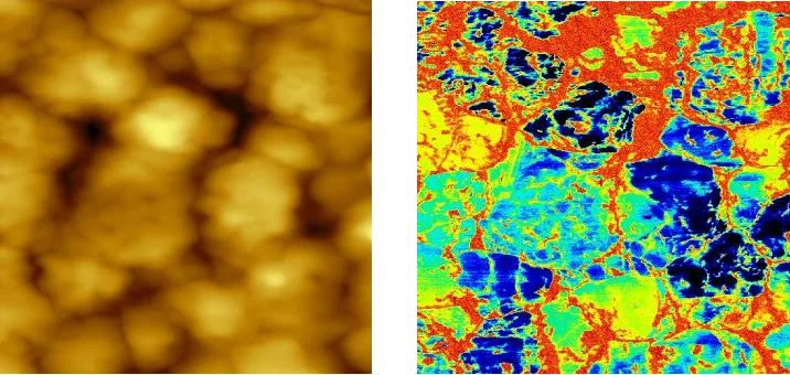
Figure 3. Perovskite solar cell resistance map. Grain-level conductivity heterogeneity revealed in a single scan pass. Dark domains indicate resistive grain boundaries; bright regions show conductive grain interiors.
Organic Solar Cells: Electrical Mapping Without Damage
Organic photovoltaic films — P3HT:PCBM, PM6:Y6, and related blends — present a particular challenge for conductive AFM: they are mechanically soft, and continuous tip-sample contact in standard C-AFM rapidly damages the organic layer, introduces friction-induced artifacts, and degrades tip conductivity. Traditional contact-mode measurements on organic PV films are therefore inherently unreliable.
Soft ResiScope™ combines Soft Interaction Control (Soft-IC) mode with ResiScope current/resistance detection. The tip makes brief, controlled vertical contacts with constant force at each pixel, retracting fully between measurements — eliminating lateral friction entirely. The result is quantitative resistance and current mapping on fragile organic films with the same 10-decade dynamic range as standard ResiScope, but without sample degradation.
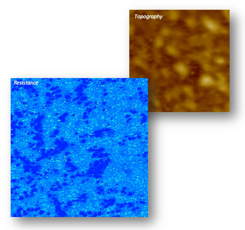
Figure 4. P3HT/PMMA organic solar cell blend — Soft ResiScope™ analysis. Phase-separated conductive (P3HT) and insulating (PMMA) domains resolved without mechanical damage to the organic film. Soft ResiScope’s friction-free interaction control preserves sample integrity across repeated scans, enabling time-series measurements on degrading organic PV films.
Choosing the Right AFM Technique for Solar Cell Research
| Technique | Measures | Best For | Key Advantage |
|---|---|---|---|
| HD-KFM III Single-pass | Surface potential, work function (mV) | Grain boundary potential, illuminated KPFM, band bending | Sub-10 nm resolution; 0.1–0.5 nm tip distance |
| Standard KFM | Surface potential (mV) | Larger-area surface potential mapping | Available on all CSI systems; simpler setup |
| ResiScope™ III 10 decades | Current (fA–μA) and resistance (10²–10¹² Ω) | Perovskite, silicon, semiconductor grain conductivity | Full dynamic range in one scan; no saturation |
| Soft ResiScope™ | Current and resistance (friction-free) | Organic PV, fragile films, repeated measurements | No sample damage; quantitative on soft materials |
| EFM | Electrostatic force gradient (qualitative) | Fast screening of charge domains | Rapid; no reference calibration needed |
| PFM / Soft PFM | Piezoelectric response | Ferroelectric domains in hybrid perovskites | Simultaneous with ResiScope III on Nano-Observer II |
Recommended Measurement Protocol
Sample Preparation in Glove Box
For air-sensitive perovskite compositions (e.g., Cs-FA mixed-halide), prepare and load samples under N₂ or Ar atmosphere. The Nano-Observer II is compatible with standard glove-box pass-through configurations. Use conductive substrates (ITO, FTO, gold) for reliable electrical contact.
Topography Survey (Resonant Mode)
Begin with a standard resonant (tapping) mode topography scan to map grain size, film roughness, and identify regions of interest. Target scan areas of 2–10 µm for grain boundary analysis. Identify representative grains of varying orientation or composition for correlation studies.
HD-KFM III — Dark Condition Surface Potential
Acquire simultaneous topography and surface potential map in single-pass HD-KFM III mode. Calibrate tip work function using a freshly cleaved HOPG reference. Record at least 3 areas per sample for statistical grain boundary potential analysis.
Illuminated KPFM — Surface Photovoltage
Repeat HD-KFM III scan on the same area under controlled white light illumination (use the Nano-Observer II optical access port). The difference map (light − dark) yields the surface photovoltage, directly measuring local charge separation efficiency at each grain and boundary.
ResiScope™ III — Resistance / Current Map
Switch to ResiScope III mode on the same or adjacent scan area. Apply a small DC sample bias (typically 0.1–0.5 V). AutoGain ensures no saturation across grain boundaries and grain interiors regardless of the resistance contrast. Correlate resistance features with KPFM potential features.
Data Correlation in NanoSolution Software
NanoSolution software enables overlay and direct pixel-by-pixel correlation of topography, surface potential, and resistance maps acquired on the same area. Export for grain boundary statistics, current pathway mapping, and comparison with macroscopic J-V device data.
Nano-Observer II — Configured for Photovoltaic Research
The Nano-Observer II combines HD-KFM III, ResiScope III, Soft ResiScope, and Soft PFM in a single platform with glove-box compatibility and optical access for illuminated experiments. Key photovoltaic-specific capabilities:
Glove Box Compatible
Full N₂/Ar atmosphere operation for air-sensitive perovskite, organic, and lithium-based samples.
Optical Coupling
Open design accepts UV, visible, and IR light sources for illuminated KPFM, surface photovoltage, and photo-conductive AFM.
Temperature Control
–40°C to 450°C with optional Peltier or heating stage — enabling stability and degradation studies under thermal stress.
Electrochemical Cell
Three-electrode EC-AFM configuration for in-situ ionic transport, corrosion, and solid-state battery interface studies.
Request a Perovskite Measurement Demo
Talk to our application specialists about KPFM and ResiScope™
measurement protocols for your specific sample and research question.
Measurement check
A known potential, measured
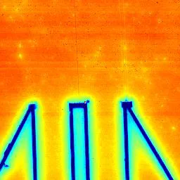
Before interpreting potential contrast on an unknown film, KPFM can be checked on a structure whose potential is set externally. With the electrodes biased, the HD-KFM map shows the applied potential as a uniform level on each electrode and how it spreads into the surrounding surface. The same HD-KFM image is shown on the HD-KFM™ III page with other reference samples.
Summary
Conclusion
HD-KFM™ III maps grain-boundary surface potential in perovskite thin films in a single pass, and repeating the scan on the same area under illumination gives the surface photovoltage. ResiScope™ III adds grain-level conductivity in perovskite films and the doped-layer interfaces of silicon cells over several orders of magnitude in one scan, while Soft ResiScope™ separates conductive and insulating domains in organic blends without damaging the film. Acquired on the same Nano-Observer II and correlated in NanoSolution, these channels link the nanoscale structure of a photovoltaic film to the potential and current that govern device performance.
Published work
Research published with CSInstruments AFMs
Peer-reviewed studies on perovskite, photoresponsive and solar-fuel materials in which CSInstruments AFMs were used. More on the publications page.
- M. Vila, J. Bartolomé, A. El Astal-Quirós, et al. Morphology engineering of MAPbBr3 thin films for enhanced lighting applications. APL Mater. 2025, 13 (7): 071109.
- M. Maniadi, K. Tieriekhov, O. Ségut, et al. From the Bulk to the Nanoscale: Strong Evolution in the Structure and Chiroptical Properties of Chiral Halide Double Perovskites. Adv. Optical Mater. 2025, 13, 2402949.
- V. Virole, N. Dabke, S. Verma, et al. Visible range photoresponse of an organic single-crystal analogue of green fluorescent protein. Nanoscale 2025, 17(14), 8614-8623.
- V. Guigoz, S. Bruyère, T. Gries, et al. Copper substitution in lanthanum-deficient LaFeO3 for enhanced solar hydrogen production. Int. J. Hydrogen Energy 2025, 148, 150072.
In this application note
AFM scans and modes in this note
- AFM scan of perovskite thin film — HD-KFM™ III surface potential: potential contrast at grain boundaries, resolved in a single pass.
- AFM scan of perovskite solar cell film — ResiScope™ resistance: resistive grain boundaries and conductive grain interiors.
- AFM scan of silicon solar cell cross-section — ResiScope™ resistance: doped layer interfaces and resistance gradients.
- AFM scan of P3HT/PMMA organic solar cell blend — Soft ResiScope™: phase-separated conductive and insulating domains, no mechanical damage.
AFM modes used
FAQ
Frequently Asked Questions
Why use KPFM for perovskite solar cell characterization?
KPFM (Kelvin Probe Force Microscopy) is the primary technique for mapping nanoscale surface potential and built-in electric fields in perovskite solar cells. It reveals grain boundary potential variations (typically 50–200 mV higher than grain interiors), local open-circuit voltage (Voc) distribution, charge trap density, and band bending at ETL/perovskite and HTL/perovskite interfaces. These measurements directly correlate with device efficiency losses and degradation mechanisms that are invisible to macroscopic characterization techniques.
What does KPFM show at grain boundaries in perovskite films?
KPFM surface potential maps of perovskite films consistently show that grain boundaries exhibit distinct potential contrast compared to grain interiors. Depending on composition and processing, grain boundaries can show positive or negative potential shifts of 50–300 mV. These variations indicate local work function differences caused by ion accumulation, defect states, or compositional segregation at grain boundaries. HD-KFM III single-pass mode on the Nano-Observer II resolves these boundary features at sub-10 nm resolution, enabling correlation with grain size, orientation, and processing conditions.
How does ResiScope AFM characterize perovskite solar cells?
ResiScope™ maps local current and resistance across the perovskite film surface at nanoscale resolution. Its 10-decade dynamic range (fA to μA, 10² to 10¹² ohms) in a single scan pass allows simultaneous visualization of both highly conductive grain cores and highly resistive grain boundaries or insulating domains — without manual gain adjustment. This is critical for perovskite because resistance variations of several orders of magnitude exist within a single 2–10 µm scan area. ResiScope measurements identify current-blocking grain boundaries, shunting pathways, and local conductivity heterogeneity that directly affect photovoltaic performance.
What AFM is best for perovskite solar cell research?
The Nano-Observer II by CSInstruments is purpose-suited for perovskite AFM research. It combines HD-KFM III (single-pass surface potential with sub-10 nm resolution) and ResiScope III (10-decade electrical mapping) in one system. Critical for perovskite work: glove-box compatibility for air-sensitive samples, optical coupling for illuminated KPFM (light-on/light-off experiments), electrochemical cell option for in-situ ionic transport studies, and temperature stage (-40°C to 450°C) for stability testing. The AutoScan software with automated approach and gain control reduces operator-induced artifacts on these sensitive films.
Can KPFM measure illuminated perovskite solar cells?
Yes. The Nano-Observer II has an open optical design that allows light illumination during KPFM measurements. Illuminated KPFM (also called surface photovoltage mapping) compares surface potential maps acquired in dark and under controlled illumination, directly revealing photogenerated carrier separation, local quasi-Fermi level splitting, and regions of charge recombination. These experiments are essential for understanding how grain boundaries act as either charge recombination centers or charge transport highways under operating conditions.
Can perovskite films be measured without exposure to air?
Yes. The recommended protocol starts with sample preparation in a glove box, and the Nano-Observer II can operate inside a glove box, so moisture- and oxygen-sensitive perovskite films are measured without exposure to air.
How are organic solar cells measured without damaging the film?
With Soft ResiScope, friction-free resistance mapping in intermittent contact. On a P3HT/PMMA blend it resolves the conductive P3HT and insulating PMMA domains without mechanical damage to the organic film.
What is the recommended AFM protocol for perovskite solar cells?
Prepare the sample in a glove box, survey the topography in resonant mode, measure the surface potential in the dark with HD-KFM III, repeat under illumination for the surface photovoltage, map resistance and current with ResiScope III, then correlate the channels in the NanoSolution software.