
Your KPFM map is
half topography.
Lift-mode KPFM measures potential on a second pass, tens of nanometres away from your film. HD-KFM™ III does it on the first pass with the tip 0.1–0.5 nm from the surface — and the Nano-Observer II lights the sample from 20° to 90° while it measures.
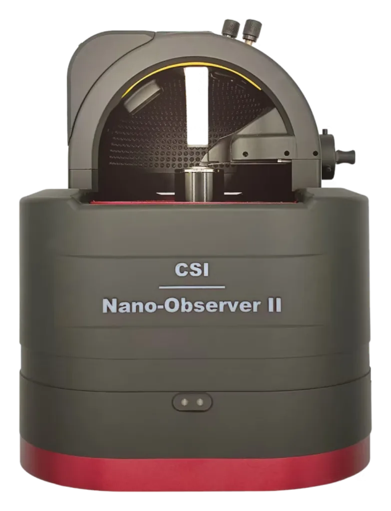
Open head · glovebox compatible
Three things that go wrong on photovoltaic films
None of them are your technique. They are limits of how a standard AFM acquires electrical data.
Potential measured from far away
A second pass at 10–100 nm lift averages the field over a large volume. Grain boundaries blur, and topographic crosstalk rides along with the potential you are trying to read.
Everything conductive reads the same
One transimpedance range cannot hold both a picoamp domain and a microamp one. The bright regions clip, a capacitive tail smears each feature along the scan line, and the surface charges as you go.
The measurement changes the sample
Dragging a biased tip across P3HT, a perovskite grain or a spin-coated blend leaves scratches — and the second scan no longer measures what the first one did.
HD-KFM™ III
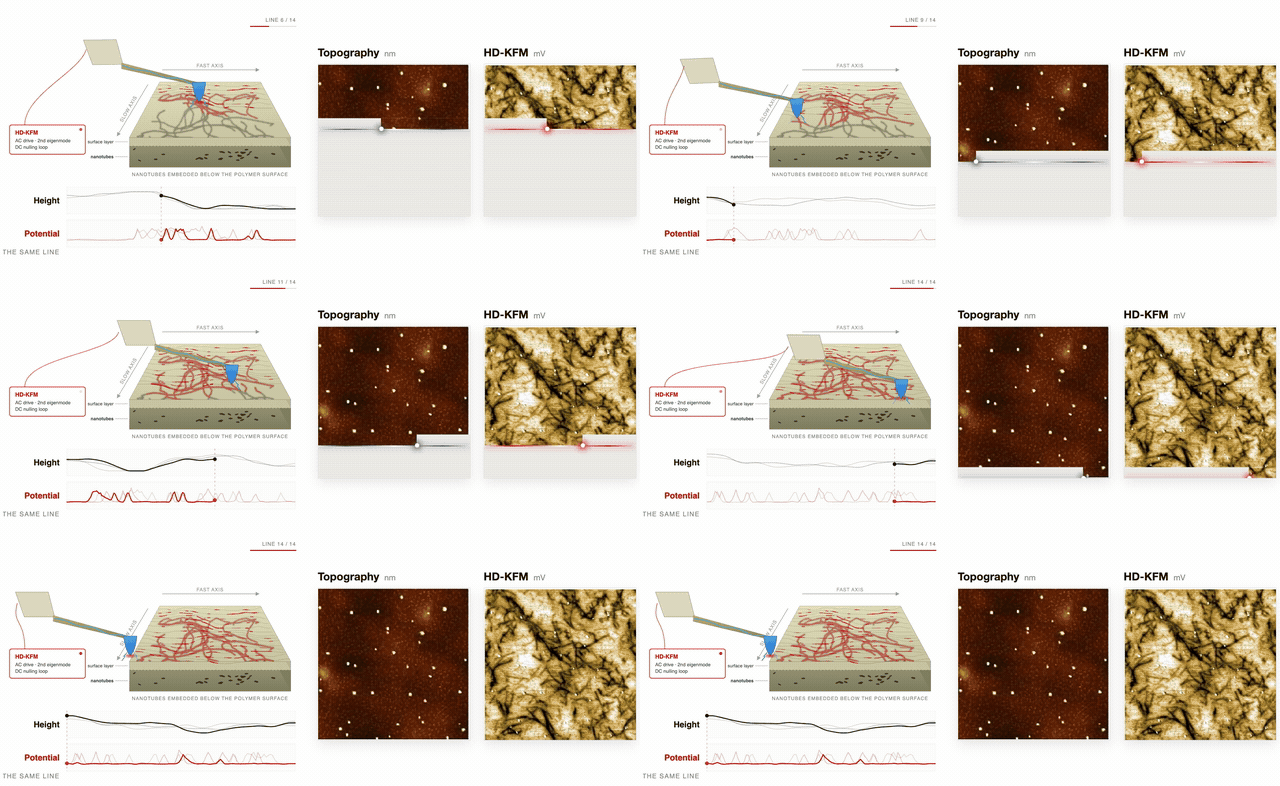
Harmonic detection on the second eigenmode of the cantilever separates the electrostatic signal from topography inside one pass. No lift, no second line — the tip stays 0.1–0.5 nm from the surface, where the field it measures is the local one.
On perovskite, grain boundaries show 50–200 mV of potential contrast, linking defect states and ion accumulation directly to efficiency loss. Sub-surface structure invisible to height shows up in potential.
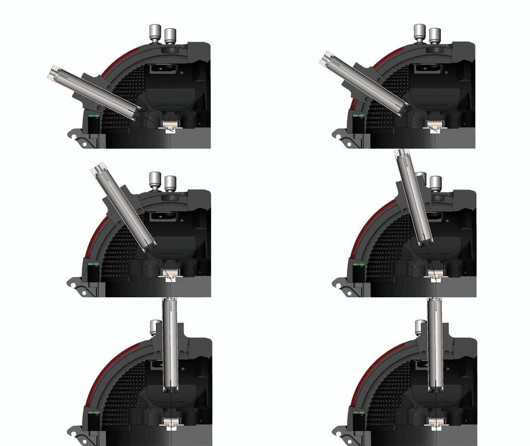
Light, from 20° to 90°
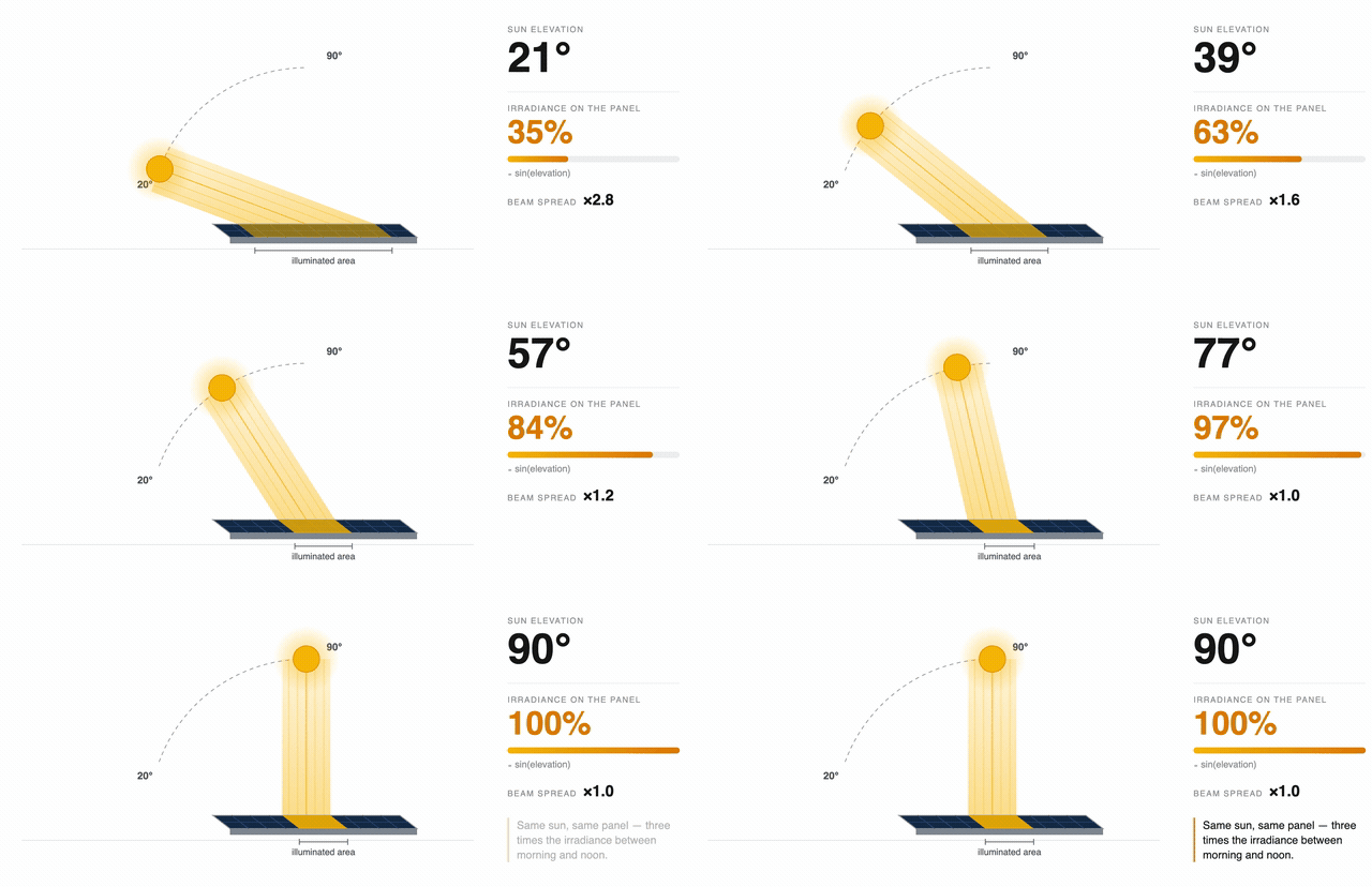
The open head takes an illumination arm on a graduated arc, locked anywhere between 20° and 90° onto the sample — the same range a panel sees over a day.
Irradiance on a flat surface follows sin(elevation): the beam keeps its width, and at low elevation the same power is spread over a larger area. Set the angle and you set the dose — then run light- and dark-KPFM on the same spot.
ResiScope™ III
A DSP-controlled auto-gain stage follows the current point by point, from 102 to 1012 Ω — picoamps and microamps in the same image, with no range switching and nothing clipped.
On soft organic films, Soft ResiScope™ lands the tip pixel by pixel: approach, hold at constant force, measure, retract, move. Zero lateral contact, so the film survives the scan.
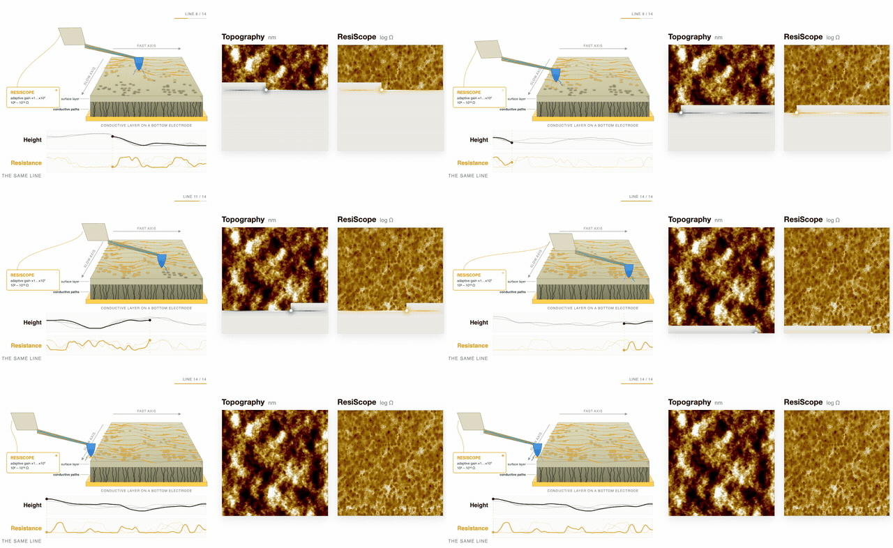

Measured on photovoltaic materials
Scans from published application studies — the same materials and the same questions your lab works on.
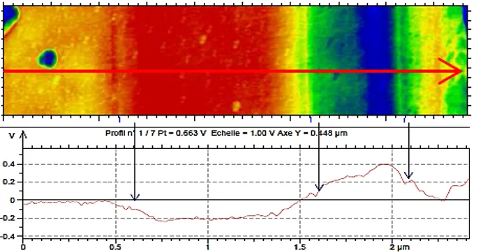
Grain-boundary potential
Single-pass surface potential across the grain structure. Boundaries carry 50–200 mV of contrast against the grain interiors.
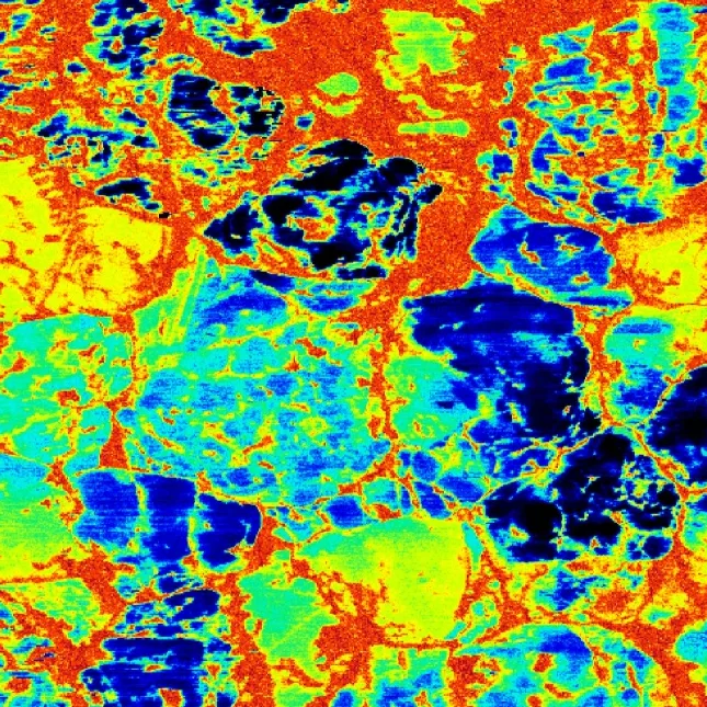
Perovskite solar cell layer
Grain morphology and local electrical response resolved on the same area, in the same session.
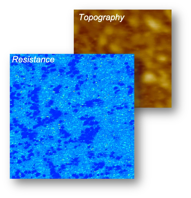
P3HT thin film
Organic semiconductor films measured without dragging the tip — Soft Interaction Control keeps the surface intact.
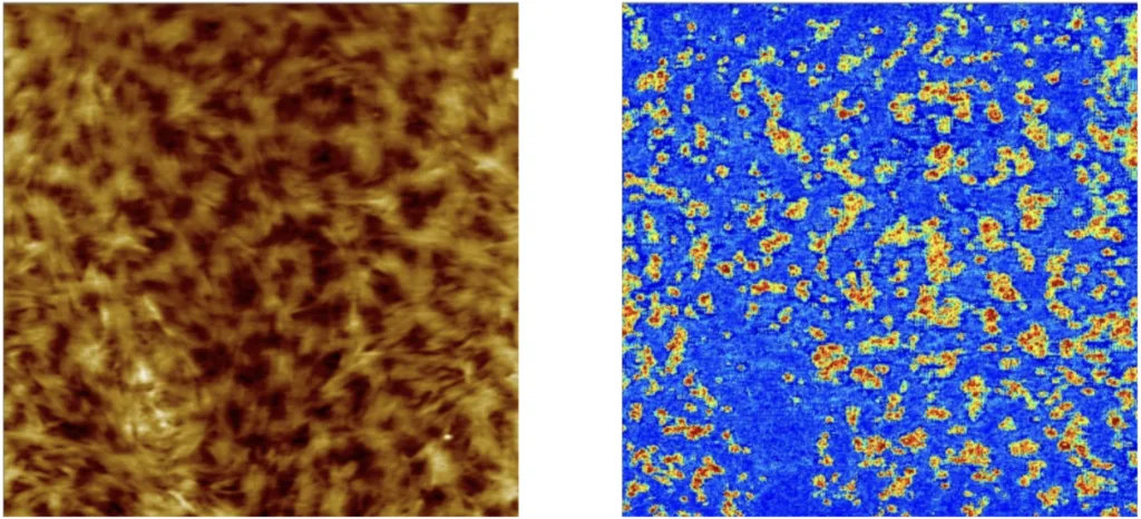
P3HT — domain structure
Phase separation and local transport in a spin-coated organic layer.
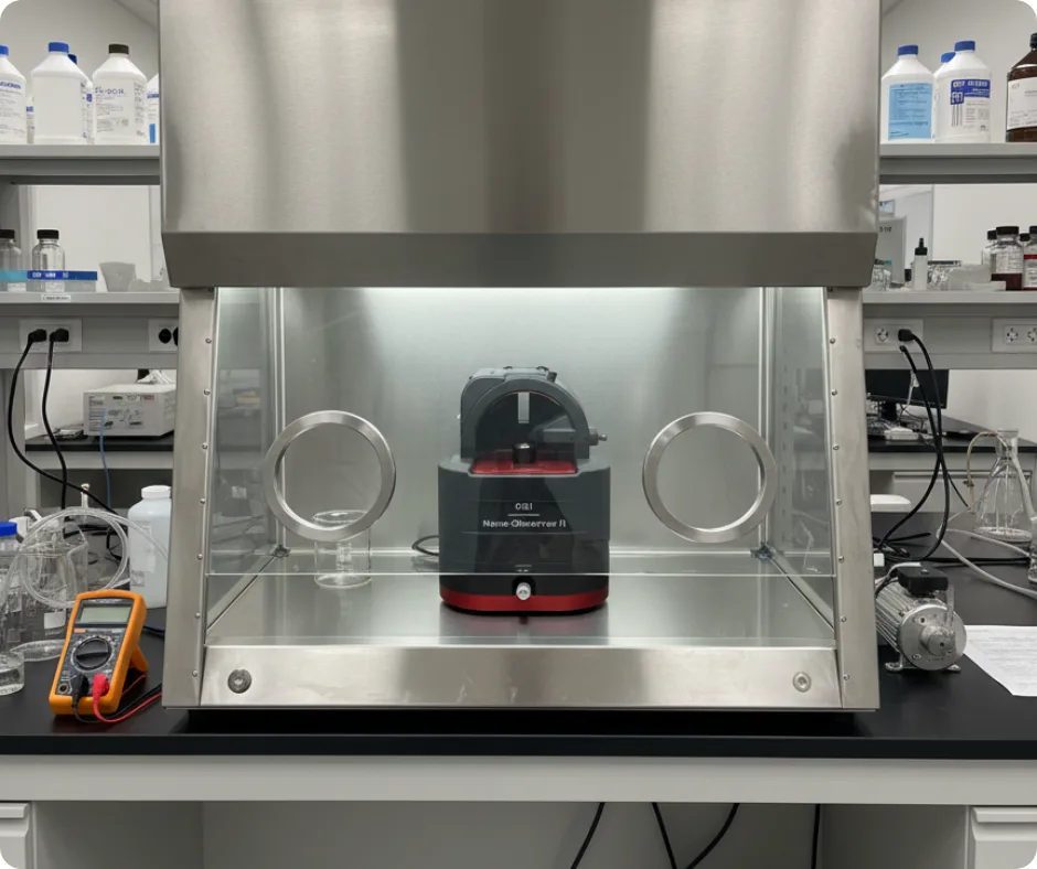
Runs inside a glovebox
Halide perovskites degrade in minutes at ambient humidity. The Nano-Observer II is compact enough to sit inside the glovebox, so the film you characterize is the film you made — with all electrical and mechanical modes still available, including illumination through the open head.
What changes on a PV sample
Where the standard technique runs out, and what replaces it.
| What you need | Standard mode | Limitation | On the Nano-Observer II |
|---|---|---|---|
| Surface potential | Lift-mode KPFM | Second pass, 10–100 nm away, topographic crosstalk | HD-KFM™ III — single pass, 0.1–0.5 nm |
| Local resistance | C-AFM | Fixed range clips; capacitive tails; surface charging | ResiScope™ III — 10² to 10¹² Ω, one scan |
| Soft organic films | Contact-mode C-AFM | Lateral force scratches the film | Soft ResiScope™ — zero lateral contact |
| Photo-response | External lamp, fixed geometry | Angle and dose not controlled or reproducible | Illumination arm — 20° to 90°, graduated |
| Air-sensitive layers | Ambient stage | Degradation during transfer and measurement | Full glovebox operation |
See it on real samples
Measurements, parameters and raw maps — not renderings.
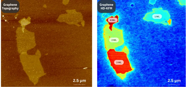
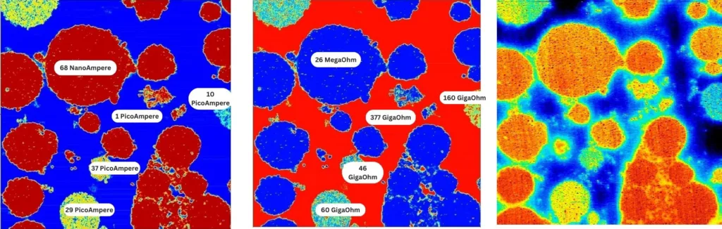
Send us a sample
Tell us what you are trying to resolve — grain boundaries, phase separation, a shunt path — and we will measure it and send you the raw data, whether or not it makes a case for the instrument.
Animated story
The same question, at the nanoscale
What a solar cell does under light depends on how the light arrives. Reproduce the angle, and you reproduce the condition — then measure the response where it happens, on the surface.
01
The same range the sun covers over a day
Irradiance follows the elevation, from 20° to 90°.
02
Reproduce the angle
…and you reproduce the condition the cell sees in the field.
03
The same sweep, on the microscope
Continuously adjustable on a graduated arc, locked at any angle onto the sample.