
Single pass
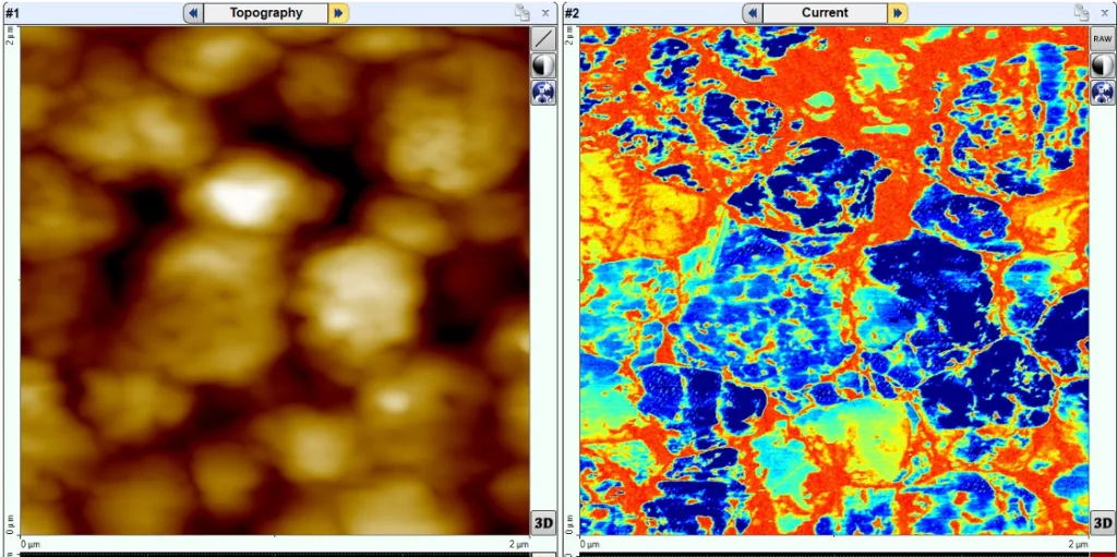
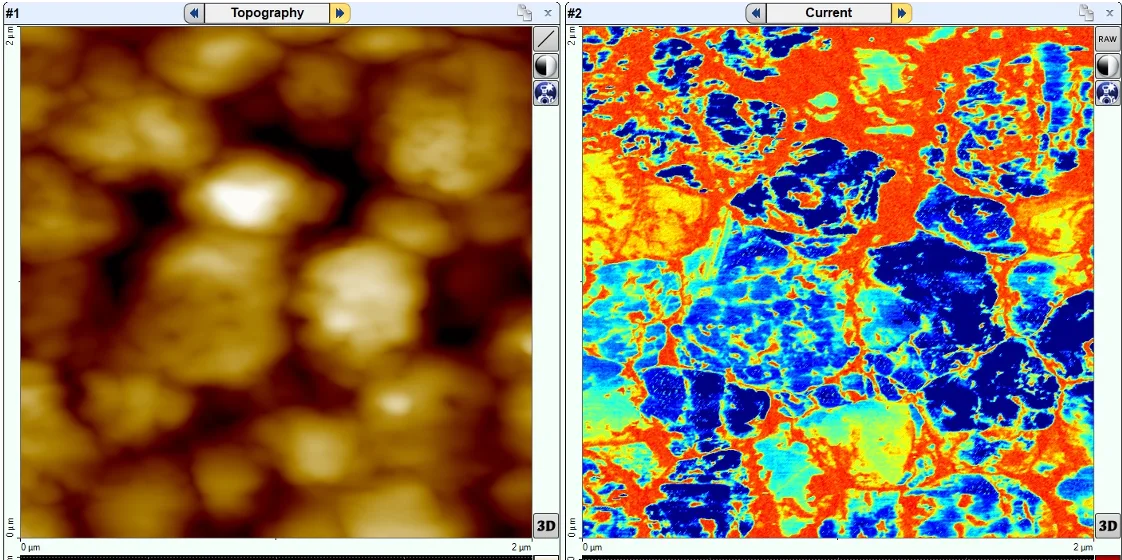
Topography and resistance, at the same time
One tip, one trajectory, one pass — both channels come out together.
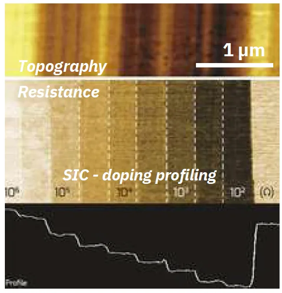
- 10 orders of magnitude in a single scan
- 10² – 10¹² Ω, no range switching by hand
- Adaptive DSP gain — no saturation, no ghost images
- Resistance and topography acquired together
Application fields
Key Features
ResiScope II
ResiScope II
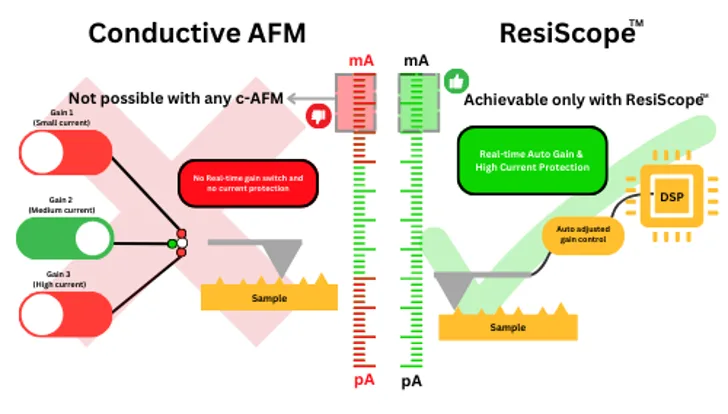
- AutoGain adjusted in real-time by ultra-fast Digital Signal Processor electronics
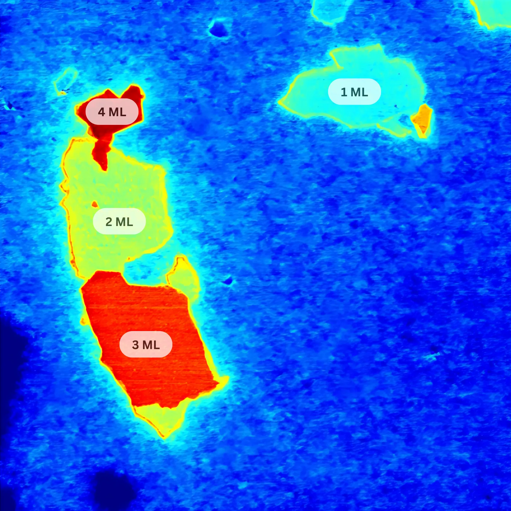
- 10 orders of magnitude range in current/resistance (fA to μA – 100 ohms to 1 Tohm)
- Both highly conductive and highly isolating domains measured in same image without user adjustment
- No logarithmic amplifiers/gains (Multiple linear gains)
- Real-time current protective integrated system
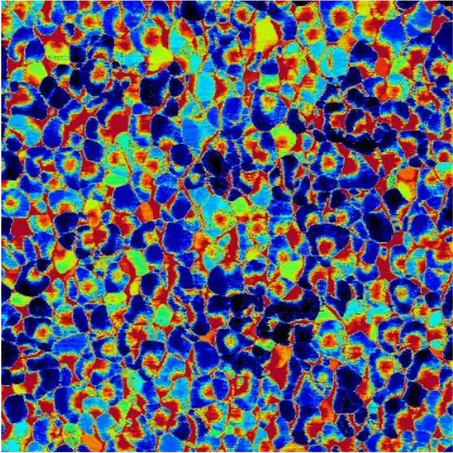
How does ResiScope™ II work?
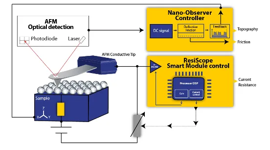
ResiScope™ II is an advanced module for Atomic Force Microscopy (AFM) that enables high-precision electrical measurements at the nanoscale. Here’s an overview of its working principle:
Conductive Probe:
- A conductive AFM tip scans the sample surface
- Tip acts as one electrode, sample as the other
Voltage Application:
- DC bias voltage applied between tip and sample
Current Measurement:
- Measures current flowing between tip and sample
- Current range: 50 fA to 1 mA
Resistance Calculation:
- Calculates local resistance using applied voltage and measured current
- Resistance range: 100 ohms to 1 Tohm
Fast Auto-Ranging:
- Processor-driven auto-ranging for real-time measurement adjustments
- No manual intervention needed
The unique design of ResiScope III allows for unprecedented sensitivity and range in electrical measurements, making it a powerful tool for nanoscale electrical characterization across a wide range of materials and applications.
Comparison with Conductive AFM
ResiScope II vs. C-AFM
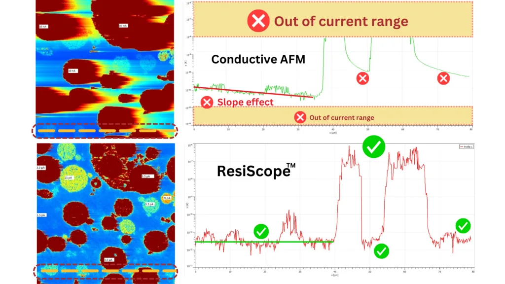
- Enhanced Visualization: Superior imaging of highly conductive areas
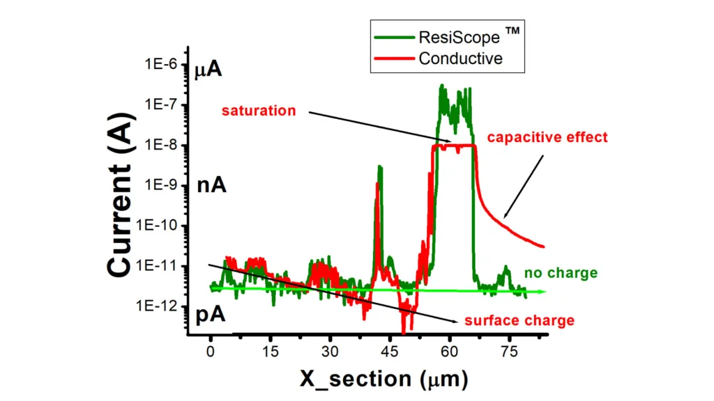
- Artifact Elimination: Avoids slope effects from surface charging
- Wider Measurement Range: 10-decade bandwidth for precise measurements
- Consistent Performance: Reliable results without capacitive discharge effects
- Comprehensive Characterization: High sensitivity for thorough electrical analysis
While traditional C-AFM remains a useful technique, ResiScope III represents a significant advancement in nanoscale electrical characterization, offering greater range, precision, and versatility for cutting-edge research and analysis.
Specifications
ResiScope Specifications
- Resistance Measurement Range: 10² to 10¹² ΩCurrent
- Measurement Range: fA to μA
- Voltage Range: ±10 V (adjustable)
- Measurement Speed: Up to 10 kHz (100 μs per measurement)
- Auto-Ranging: Real-time, processor-driven
- Current Control: Active, real-time adjustment
- Noise Level: < 10 fA RMS
- Compatible AFM Modes: Contact Mode Oscillating Mode Force Spectroscopy
- Integration Capabilities: HD-KFM MFM/EFM PFM Environmental Compatibility:Air Controlled Atmospheres Liquids
- Topography Acquisition: Simultaneous with electrical measurements
- Data Output: Real-time resistance and current mapping
- Spatial Resolution: Dependent on AFM tip radius (typically < 10 nm)
- Software: Integrated with Nano-Observer II control software
- Data Analysis: Built-in analysis tools for electrical property mapping
- Compatible Probes: Wide range of commercially available conductive AFM probes
- Scan area: Up to 100 μm x 100 μm
- Operating Temperature: 10°C to 40°C (standard), extended range available
- Humidity Range: < 80% RH, non-condensing
- Note: Exact specifications may vary depending on the AFM system and environmental conditions. Please consult with a CSInstruments representative for detailed information tailored to your specific application needs.
Application Fields
- Semiconductor Analysis (doping profiling, defect analysis, 2D semiconductors, junction studies)
- Nanoelectronics Research (nanowires, nanotubes, graphene, quantum dots, molecular electronics)
- Material Science (conductive materials, composites, corrosion studies, novel materials)
- Polymer and Composite Studies (conductive polymers, blends, carbon nanotube composites, organic electronics)
- Thin Film Characterization (uniformity analysis, dielectric films, TCO films, solar cell materials)
- Energy Materials (battery electrodes, fuel cells, photovoltaics, thermoelectrics)
- Biomaterials and Bioelectronics (conductive biomaterials, neural interfaces, biosensors)
- Advanced Coatings (anti-static coatings, conductive coatings, smart coatings)
- Memory and Data Storage (RRAM, magnetic media, phase-change memory, spintronics)
- Optoelectronics (photodetectors, LEDs, OLEDs, photovoltaic junctions)
Comparison: ResiScope™ & C-AFM
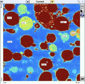
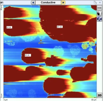
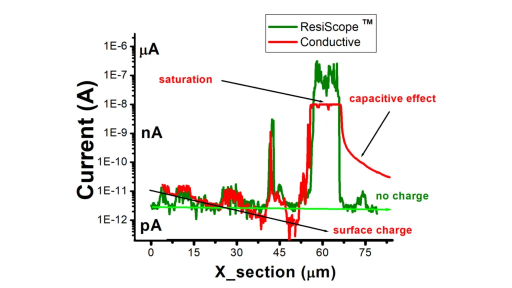
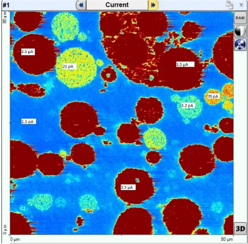
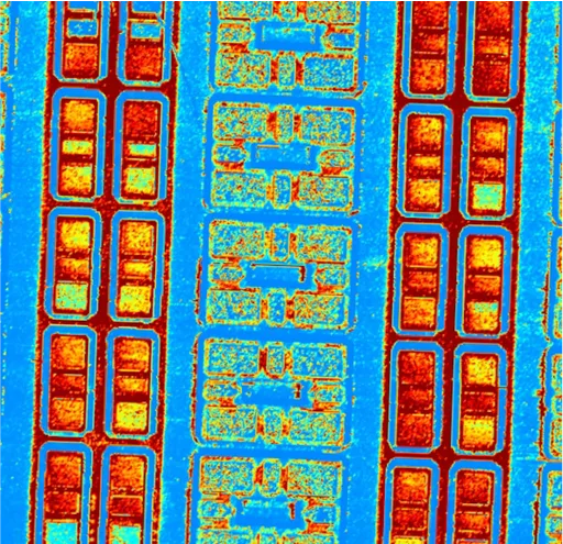
A comparative 80×80 µm scan of a polymer battery sample reveals ResiScope’s significant advantages over traditional Conductive AFM:
- Enhanced Visualization: ResiScope provides superior imaging of highly conductive areas, offering a more accurate conductivity map.
- Elimination of Artifacts: Unlike Conductive AFM, ResiScope avoids slope effects from surface charging or tip-sample interactions, ensuring data accuracy.
- Wider Measurement Range: ResiScope’s 10-decade bandwidth captures both low and high conductivity features precisely, outperforming Conductive AFM’s limited range.
- Consistent Performance: ResiScope maintains reliable results without the capacitive discharge effects observed in Conductive AFM after scanning highly conductive regions.
- Comprehensive Characterization: ResiScope’s high sensitivity and precision make it the superior tool for thorough electrical characterization of complex materials like polymer batteries.
In summary, ResiScope offers more accurate, comprehensive, and reliable electrical measurements, particularly crucial for advanced materials research and development.
Application note
ResiScope™ in battery research
Conductivity mapping of battery materials with ResiScope™, with the measurement set-up and results.
Dynamic range
Conductive AFM vs ResiScope™
Conductive AFM works with one gain, fixed before the scan: only one window is measured correctly. ResiScope™ re-chooses the gain at every measured point.
- Every decade from pA to µA in one scan
- No saturation above the range, no signal lost in noise below it
- Real-time auto gain and high-current protection for tip and sample
Product note
ResiScope™ II product note
Principle, key specifications and application examples in one technical document. We send it to you by e-mail.
Questions about ResiScope™?
Ask the application scientists behind our AFMs and modes — about your samples, probes, set-up or which mode fits your measurement. We answer every message personally.