
Key takeaways
- HD-KFM™ surface potential resolves triangular moiré domains of about 100 nm in folded hBN at a 1 µm scan — invisible in the topography.
- Graphene layers from one to four monolayers are distinguished by work-function contrast, with sharp interfaces.
- On few-layer MoS₂, work function (HD-KFM™) and resistance (ResiScope™) are mapped on the same area.
- HD-KFM™ is single-pass KPFM: no lift artefacts, second-eigenmode detection, electric field cancelling (EFC) and one-click setup.
Single pass
Topography and surface potential, at the same time
One tip, one trajectory, one pass — both channels come out together.
- Single pass — no lift, no second line
- 2nd eigenmode harmonic detection
- Tip stays 0.1–0.5 nm from the surface
- Potential contrast at the resolution of the topography
- Sub-surface detection — structures buried under the surface (e.g. nanotubes in a polymer)
Why 2D Materials Demand Nanoscale Electrical Characterization
The electronic properties of graphene, hBN, and MoS₂ are exquisitely sensitive to layer count — a single additional atomic layer can shift the work function by tens of millivolts, switch a semiconductor to a semimetal, or introduce moiré-driven quantum phenomena that exist at no other length scale.
Conventional optical and transport measurements provide spatially averaged information. They cannot identify where charge accumulates, how domains interact, or what happens at a twisted bilayer interface. Kelvin Force Microscopy (KFM) and conductive AFM provide the missing spatial dimension — mapping potential and conductivity distributions with sub-10 nm resolution across the exact grain and domain structures responsible for device-level behavior.
Hexagonal Boron Nitride: Moiré Pattern Visualization
Folded or twisted hBN layers form moiré superlattices — periodic interference patterns arising from rotational misalignment between atomic planes. These superlattices create long-range modulations in local electronic structure and are central to engineered quantum materials. HD-KFM maps the charge and potential modulations of moiré domains with the resolution needed to characterize them.
The Nano-Observer AFM with HD-KFM provides multi-scale characterization of folded hBN across three complementary length scales, revealing the complete hierarchy of structural and electronic organization in a single session:
| Scale | What is mapped | Key information |
|---|---|---|
| 5 µm scan | Large-scale domain structure | Overall sample architecture, folded region geometry, domain size distribution |
| 2 µm scan | Mid-range domain boundary mapping | Boundary sharpness, transition widths, lateral potential gradients between domains |
| 1 µm scan | High-resolution moiré visualization | ~100 nm triangular moiré domains, intralayer charge modulation, twist-angle dependent periodicity |
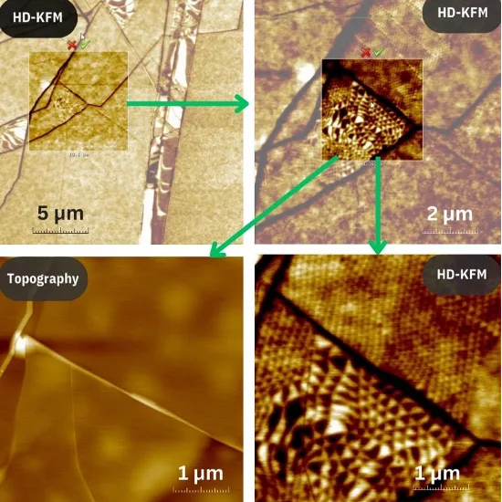
Figure 1. Multi-scale HD-KFM surface potential maps of folded hBN. At 1 µm resolution, triangular moiré domains of approximately 100 nm are clearly resolved through periodic surface potential modulation — invisible to topography alone. Nano-Observer AFM.
Graphene: Layer-by-Layer Work Function Mapping
Graphene’s electronic properties depend critically on layer count. Monolayer graphene is a zero-gap semimetal with linear Dirac dispersion; bilayer graphene has a parabolic band structure and a tunable bandgap; trilayer and thicker films shift toward graphite-like behavior. Identifying these regions spatially is a fundamental requirement for 2D materials research and device fabrication.
Each additional graphene layer produces a measurable, systematic shift in local surface potential, creating distinct color contrast in the KFM map that enables unambiguous layer assignment — simultaneously with topography acquisition.
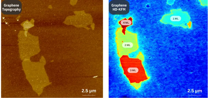
Figure 2. Correlated topography and HD-KFM surface potential map of multi-layer graphene. Layer regions 1ML through 4ML are unambiguously distinguished by work function contrast, with sharp, well-defined interfaces visible in both channels. Nano-Observer AFM.
Monolayer Identification
Lowest work function region with maximum substrate influence. Distinct potential contrast vs. the SiO₂ substrate enables unambiguous 1ML assignment.
Bilayer & Trilayer Contrast
Intermediate work function shifts with progressively reduced substrate screening. Bernal vs. twisted stacking distinguishable in the 3ML region.
Interface Sharpness
Sharp, well-defined boundaries between layer count regions — directly revealing flake geometry and edge structure at sub-10 nm resolution.
Substrate Effects
hBN substrates reduce charge inhomogeneity in graphene layers. Molecular intercalation (water, oxygen) modifies work functions and is detectable by HD-KFM.
MoS₂: Combined Work Function and Resistance Mapping
Molybdenum disulfide (MoS₂) is a transition metal dichalcogenide (TMD) with a dramatic layer-dependent electronic transition: bulk MoS₂ is an indirect bandgap semiconductor (1.2 eV), while monolayer MoS₂ becomes a direct bandgap semiconductor (1.8 eV) with strong photoluminescence. This transition is accompanied by measurable changes in both surface potential and electrical conductivity.
The combination of HD-KFM and ResiScope™ is uniquely powerful for TMD characterization because the two measurements are complementary and non-redundant. Work function (HD-KFM) reflects changes in electrostatic potential and band alignment; resistance (ResiScope™) reflects carrier density and mobility. Together, they provide a complete picture of how the semiconductor-to-semimetal transition in MoS₂ evolves at the single-layer level.
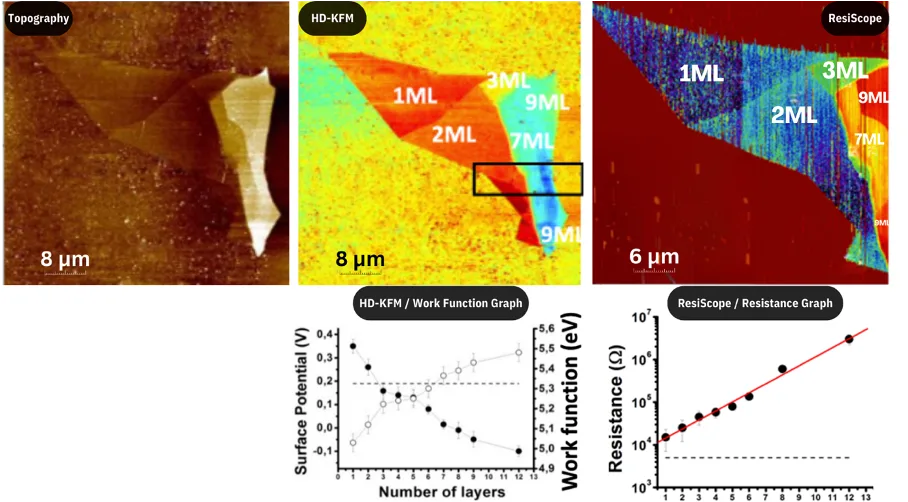
Figure 3. Correlated topography, HD-KFM surface potential, and ResiScope™ resistance maps of few-layer MoS₂, with accompanying quantitative line profiles. The resistance map reveals exponential conductivity changes across layer boundaries — data inaccessible to either technique alone. Nano-Observer AFM.
HD-KFM — Work Function
- Maps work function shifts with nanometer-scale resolution
- Reveals charge distribution across different layer counts
- Shows systematic surface potential changes with layer thickness
- Detects interlayer charge transfer at domain boundaries
ResiScope™ — Resistance
- Maps resistance across 10² to 10¹² Ω in a single scan
- Distinguishes conductive and insulating regions clearly
- Quantifies exponential conductivity change with layer count
- No manual gain adjustment — full range captured automatically
HD-KFM: Harmonic Detection Kelvin Force Microscopy
HD-KFM (Harmonic Detection Kelvin Force Microscopy) is CSInstruments’ proprietary single-pass KFM implementation. Unlike conventional dual-pass (lift mode) KPFM, HD-KFM measures topography and surface potential simultaneously in a single scan — eliminating tip-sample distance drift artifacts that degrade resolution in two-pass measurements.
By leveraging the cantilever’s second eigenmode through harmonic detection, HD-KFM operates at high frequency (~350–400 kHz), enabling not only high-resolution surface potential mapping but also sensitivity to sub-surface features and buried interfaces invisible to conventional KFM techniques.
Single Pass — No Lift Artifacts
Topography and surface potential acquired simultaneously. No tip-sample distance drift between passes — sharper boundaries, more accurate potential values.
Second Eigenmode Detection
High-frequency (~350–400 kHz) harmonic operation delivers 20–30× more detection cycles per pixel than conventional side-band KFM, significantly improving signal-to-noise ratio.
Electric Field Cancelling (EFC)
EFC enables pure MFM measurements by eliminating unwanted electrostatic contributions — essential for samples with both magnetic and electrical properties.
One-Click Setup
Built-in auto-tune algorithm optimizes all settings automatically. No multi-step manual adjustment required — reproducible results across operators and sessions.
Characterize Your 2D Materials with HD-KFM
Contact our application specialists to discuss your graphene, hBN, or TMD characterization requirements — or request application data for your specific material system.
Measurement check
A known potential, measured
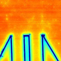
Before interpreting potential contrast on an unknown film, KPFM can be checked on a structure whose potential is set externally. With the electrodes biased, the HD-KFM map shows the applied potential as a uniform level on each electrode and how it spreads into the surrounding surface. The same HD-KFM image is shown on the HD-KFM™ III page with other reference samples.
Summary
Conclusion
HD-KFM™ records topography and surface potential in the same single pass, which resolves about 100 nm triangular moiré domains in folded hBN, distinguishes graphene from one to four layers by work-function contrast and, combined with ResiScope™, maps layer-dependent work function and resistance on few-layer MoS₂. Because the channels are acquired on the same area, layer number, potential and conductivity can be compared directly on one Nano-Observer AFM.
Published work
Research published with CSInstruments AFMs
Peer-reviewed studies on 2D materials and graphene-based nanostructures in which CSInstruments AFMs were used. More on the publications page.
- M. C. Giordano, G. Zambito, M. Gardella, F. B. de Mongeot Deterministic Thermal Sculpting of Large-Scale 2D Semiconductor Nanocircuits. Advanced Materials Interfaces 2022, 10 (5), 2201408.
- G. Zambito, G. Ferrando, M. Barelli, et al. Thermomechanical Nanostraining of Two-Dimensional Materials. Small Science 2026, e202500404.
- S. Elsayed, H. H.D. AlTakroori, M. U. Khan, et al. Near-infrared photosensors based on uniform 2D carbon nanotube networks. Diamond and Related Materials 2025, 158, 112663.
- R. Sainz, M. del Pozo, M. Vilas-Varela, et al. Chemically synthesized chevron-like graphene nanoribbons for electrochemical sensors. Sci. Rep. 2020, 10, 14614.
- C. Pardanaud, A. Campos, et al. Tape's Crucial Role in Optimizing Mechanical Exfoliation of Large-Scale Rhombohedral Graphene. SSRN preprint 2025.
In this application note
AFM scans and modes in this note
- AFM scan of folded hexagonal boron nitride (hBN) — HD-KFM™, 5, 2 and 1 µm: moiré superlattice domains of about 100 nm.
- AFM scan of multi-layer graphene — topography + HD-KFM™ surface potential: layers from 1 ML to 4 ML by work function.
- AFM scan of few-layer MoS₂ — topography, HD-KFM™ and ResiScope™: work function and resistance with line profiles.
AFM modes used
FAQ
Frequently Asked Questions
Why use KPFM for 2D material characterization?
Kelvin Force Microscopy (KFM) is the primary AFM technique for characterizing the electronic properties of 2D materials such as graphene, hBN, and MoS₂. It directly maps surface potential and work function at nanometer resolution, revealing layer-dependent electronic structure, moiré superlattice charge modulation, and interfacial charge transfer effects that are invisible to topography imaging alone. In single-pass HD-KFM mode, the technique achieves sub-10 nm spatial resolution with minimal electrostatic tip-sample perturbation, making it ideal for ultrathin van der Waals heterostructures.
How does AFM reveal moiré patterns in hBN?
Moiré patterns in folded or twisted hBN arise from periodic lattice interference between misaligned layers, creating superlattice modulations on the 10–100 nm scale. HD-KFM surface potential mapping on the Nano-Observer AFM resolves these features at multiple scales: large-scale domain structure (5 µm scale) showing overall architecture, mid-range mapping (2 µm scale) of domain boundaries and transitions, and high-resolution moiré pattern visualization with ~100 nm triangular domains at 1 µm scale. The surface potential contrast in HD-KFM directly reflects local variations in interlayer coupling and charge redistribution across the moiré unit cell.
Can AFM distinguish graphene monolayer from bilayer and trilayer?
Yes. HD-KFM on the Nano-Observer AFM distinguishes monolayer (1ML), bilayer (2ML), trilayer (3ML), and four-layer (4ML) graphene regions through work function contrast in the surface potential map. Each additional graphene layer produces a measurable, systematic shift in local surface potential, creating distinct, reproducible color contrast in the KFM image. The technique simultaneously maps sharp, well-defined interfaces between regions with different layer counts and correlates electronic structure directly with topographic layer thickness measurements.
How is MoS₂ characterized by AFM?
MoS₂ characterization on the Nano-Observer AFM combines HD-KFM and ResiScope™ for comprehensive layer-dependent analysis. HD-KFM maps work function shifts with nanometer-scale resolution, reveals charge distribution across different layer counts, and shows systematic changes in surface potential with layer thickness. ResiScope™ maps resistance across an exceptional 10-decade dynamic range (10² to 10¹² Ω), clearly distinguishing conductive and insulating regions and quantifying how conductivity changes exponentially with the number of MoS₂ layers.
What is HD-KFM and how does it differ from standard KPFM?
HD-KFM (Harmonic Detection Kelvin Force Microscopy) is CSInstruments' proprietary single-pass KFM implementation. Unlike conventional dual-pass (lift mode) KPFM, HD-KFM measures topography and surface potential simultaneously in a single scan, eliminating tip-sample distance drift artifacts. The harmonic detection approach leverages the cantilever's second eigenmode at high frequency (~350–400 kHz), achieving sub-10 nm lateral resolution.
What AFM is best for graphene and 2D materials research?
The Nano-Observer AFM with HD-KFM module is optimized for 2D materials characterization. Its single-pass KFM implementation provides the spatial resolution necessary to map moiré superlattices, layer boundaries, and interlayer charge transfer in van der Waals heterostructures. The optional ResiScope™ module extends characterization to resistance mapping across 10 decades (10² to 10¹² Ω), enabling correlated work function and conductivity measurements on the same sample area.
Are moiré patterns visible in AFM topography?
Not on the folded hBN of this note: the surface is atomically flat, and the triangular moiré domains of about 100 nm appear only in the HD-KFM surface-potential channel.
What scan size is needed to resolve moiré domains in hBN?
In this note the multi-scale series goes from 5 µm to 2 µm to 1 µm; the moiré domains of about 100 nm are clearly resolved at the 1 µm scan size.