
AFM for 2D materials
Which AFM for graphene, hBN and MoS₂?
Topography alone says little about a 2D material: one extra atomic layer changes the work function and the conductivity, and moiré superlattices can be invisible in height images. What matters is electrical contrast at nanometre resolution. The Nano-Observer II AFM from CSInstruments combines the modes that give it on the same sample:
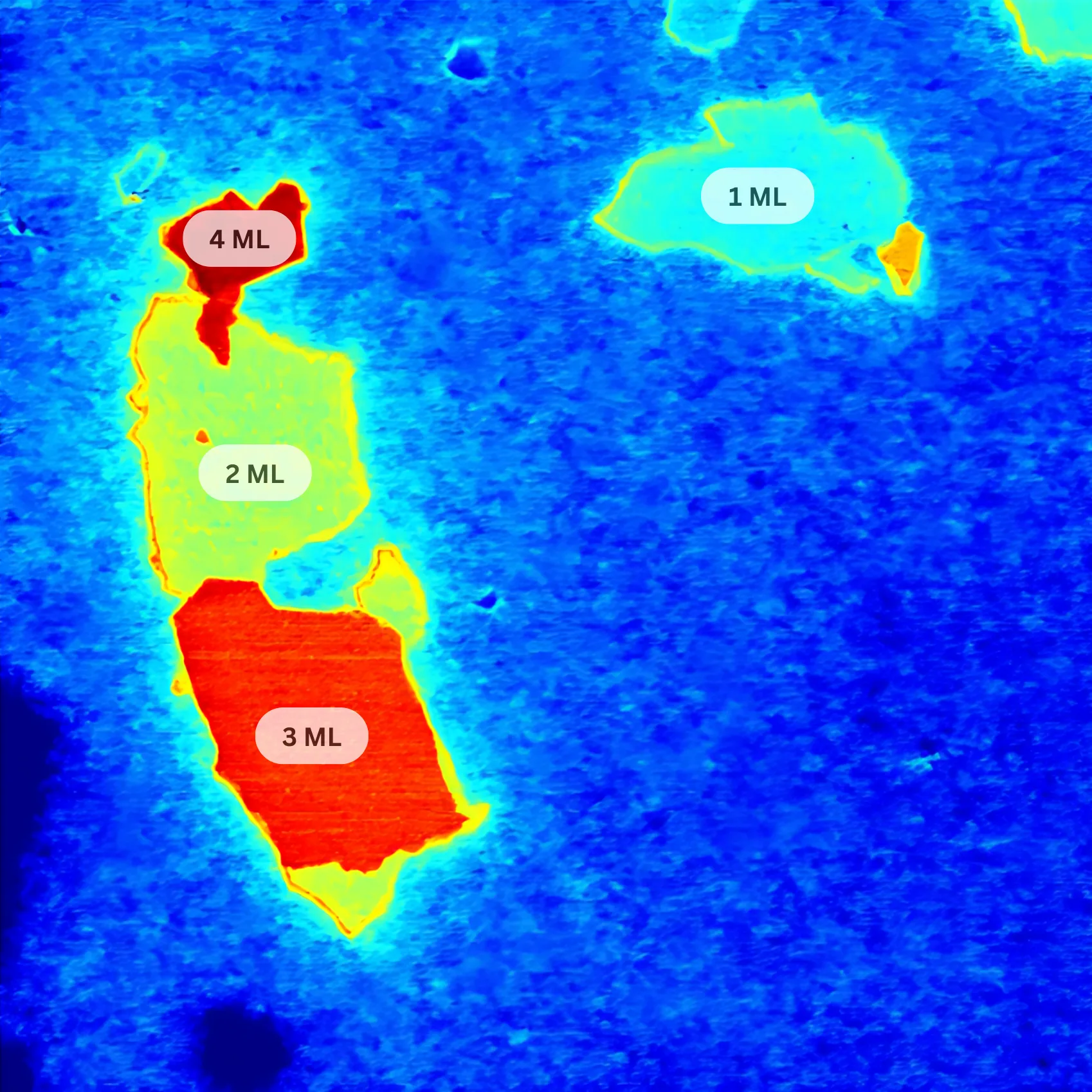
- Layer counting and work function — HD-KFM™, single-pass Kelvin probe force microscopy (KPFM), distinguishes graphene from one to four monolayers.
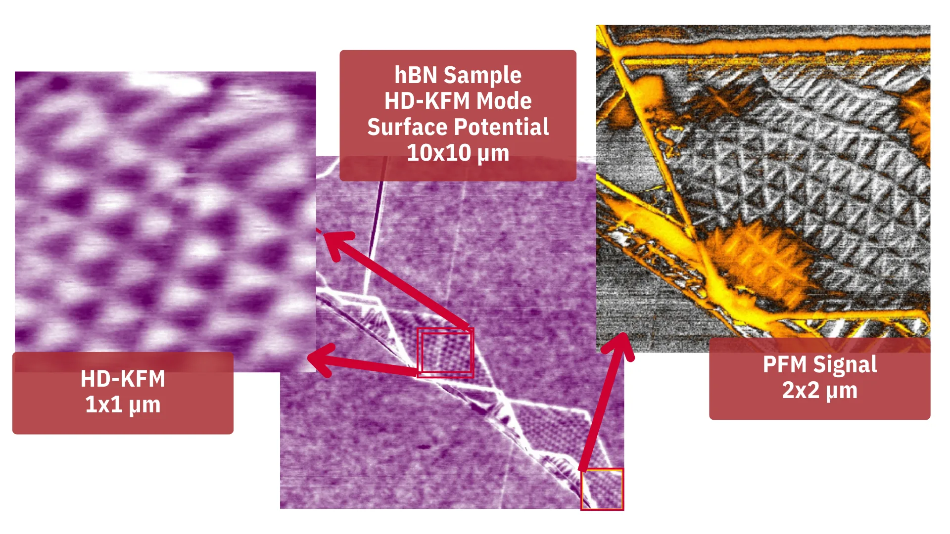
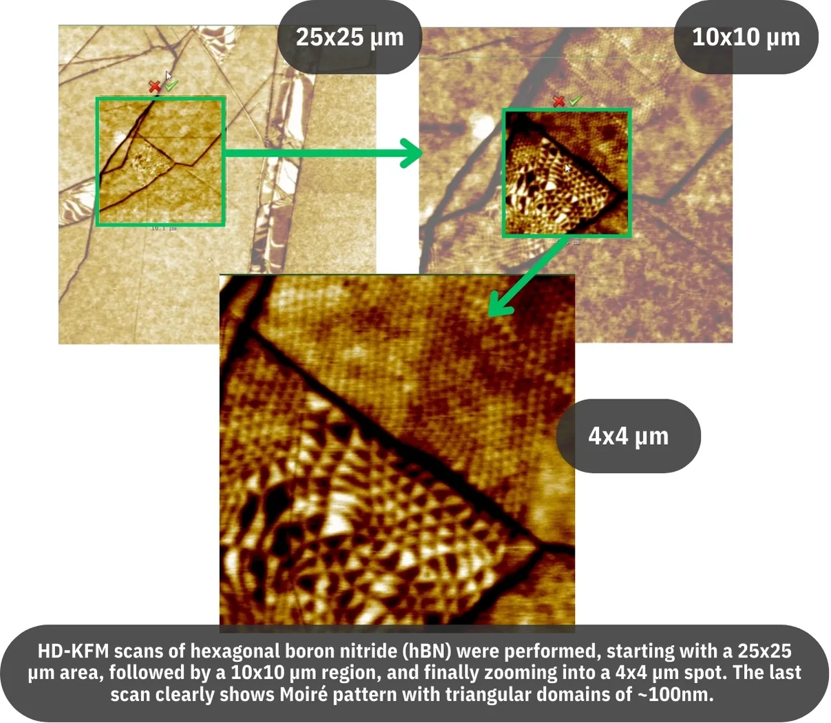
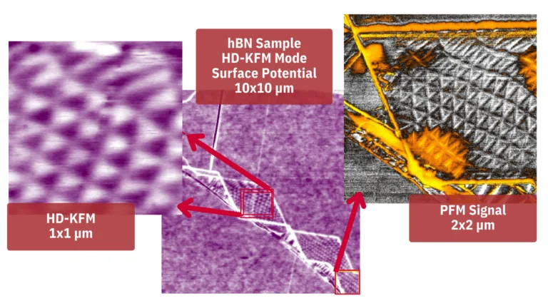
- Moiré domains — in folded hBN, HD-KFM™ resolves triangular domains of about 100 nm at a 1 µm scan, while the topography is atomically flat; PFM shows the same pattern.
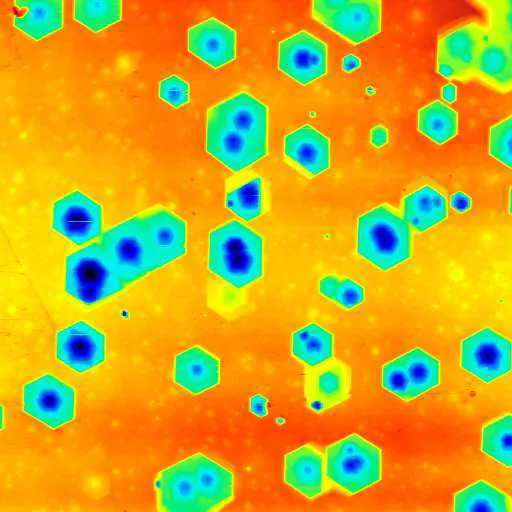
- Conductivity — ResiScope™ maps resistance over 10 decades; on few-layer MoS₂ it is recorded on the same area as the work function.
- Flakes on a substrate — resonant-mode phase separates graphene flakes from the SiO₂ underneath.
Images
Videos
Application Notes – 2D Materials
HD-KFM & AFM Characterization of 2D Materials
Explore HD-KFM & AFM Characterization of 2D Materials, revealing nanoscale electronic structures in graphene and MoS₂. Discover HD-KFM & AFM insights now!
Read more: HD-KFM & AFM Characterization of 2D Materials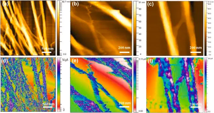
Engineering Selective Terahertz Photodetection
Conductive AFM validates CNT conductivity in selective THz photodetectors. Nanoscale current mapping of carbon nanotube rectennas.
Read more: Engineering Selective Terahertz Photodetection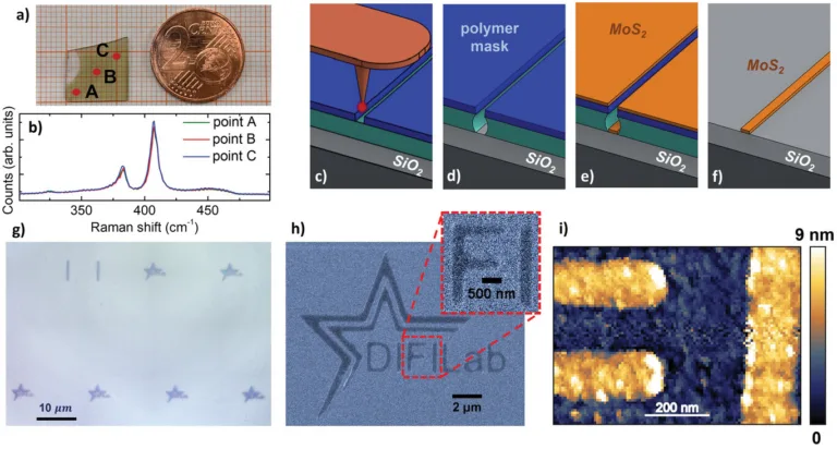
Scalable 2D Semiconductor Nanocircuits
Scalable 2D semiconductor nanocircuits: HD-KFM & ResiScope characterization of MoS₂ nanopaths with CSI Nano-Observer AFM. University of Genoa research.
Read more: Scalable 2D Semiconductor Nanocircuits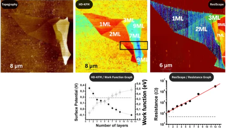
ResiScope™ III: Revolutionary Nanoscale Electrical Characterization for Advanced Materials Research
Discover advanced Conductive AFM technology with ResiScope III. Achieve nanoscale electrical characterization with 10 orders of magnitude range, real-time adaptive electronics, and artifact-free measurements for solar…
Read more: ResiScope™ III: Revolutionary Nanoscale Electrical Characterization for Advanced Materials Research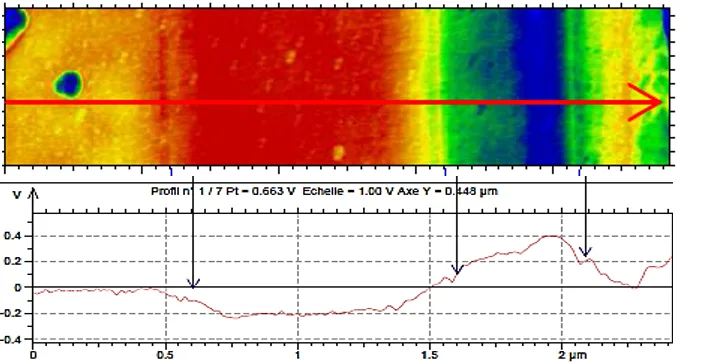
Nanoscale AFM Breakthrough: Advanced Characterization Techniques for Next-Generation Solar Cells
Explore revolutionary HD-KFM™, ResiScope™, and Soft IC Mode technologies for characterizing organic and perovskite solar cells. Discover how nanoscale AFM analysis accelerates photovoltaic innovation.
Read more: Nanoscale AFM Breakthrough: Advanced Characterization Techniques for Next-Generation Solar Cells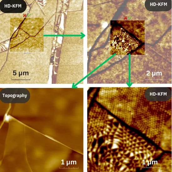
Unlocking the Nanoscale: How HD-KFM Technology is Revolutionizing 2D Materials Characterization
Discover how High-Definition Kelvin Probe Force Microscopy (HD-KFM) enables breakthrough characterization of graphene, MoS₂, and hBN at the atomic scale. Learn about advanced AFM techniques transforming…
Read more: Unlocking the Nanoscale: How HD-KFM Technology is Revolutionizing 2D Materials CharacterizationFAQ
Frequently Asked Questions
What is the best AFM technique for graphene and other 2D materials?
Electrical AFM modes, because the layer number and stacking of 2D materials show up in the work function and the conductivity more than in the topography. Single-pass KPFM (HD-KFM) maps the work function, ResiScope maps resistance and PFM maps polarization domains; the Nano-Observer II combines them on the same sample.
Can AFM count the number of graphene layers?
Yes. HD-KFM surface potential distinguishes graphene regions from one to four monolayers by their work function, with sharp interfaces between layers.
Can AFM image moiré patterns in hBN?
Yes, in the surface-potential channel. HD-KFM resolves triangular moiré domains of about 100 nm in folded hBN at a 1 µm scan, while the topography is atomically flat. PFM shows the same moiré pattern.