Non-Invasive Additive Nanofabrication & Multi-Modal Electrical Nanoscopy
The Challenge of 2D Semiconductor Nanofabrication
Two-dimensional transition metal dichalcogenides (TMDs) like MoS₂ hold enormous promise for next-generation nanoelectronics and photonics. However, integrating these atomically thin materials into functional nanocircuits requires:
- Large-scale uniform growth (cm² substrates)
- Nanoscale patterning without contamination or damage
- Preservation of semiconducting properties
- Deterministic placement and geometry control
Traditional subtractive approaches using reactive ion etching introduce contamination and surface damage to fragile 2D layers. The work by Giordano et al. at the University of Genoa demonstrates a breakthrough additive approach.
Additive Nanolithography: t-SPL + Large-Area Deposition
The researchers combined two key innovations:
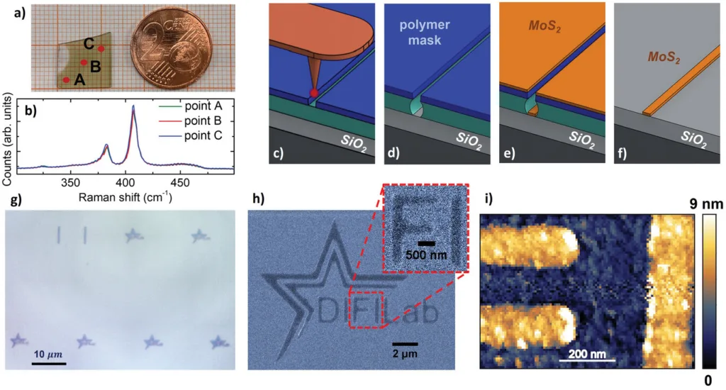
1. Ion Beam-Assisted Physical Deposition: Homogeneous few-layer MoS₂ films grown across entire substrates via collimated ion beam sputtering of stoichiometric MoS₂ targets. Room-temperature deposition followed by 750°C sulfurization yields high-quality 2H-semiconducting phase.
2. Thermal-Scanning Probe Lithography (t-SPL): Non-invasive nanopatterning of sacrificial polymer bilayers creates negative-angle masks. Subsequent MoS₂ growth and lift-off produces clean, precisely positioned nanocircuits down to 130 nm width.
This additive method avoids plasma exposure or chemical etching, preserving the pristine electronic properties of the 2D semiconductor while enabling arbitrary geometries across large areas.
Raman Confirmation of Semiconducting Phase
Micro-Raman spectroscopy confirmed the characteristic E¹₂g (383 cm⁻¹) and A₁g (408 cm⁻¹) vibrational modes of few-layer 2H-MoS₂. The homogeneous Raman maps across entire nanocircuits demonstrated structural integrity and phase purity.
Electrical Nanoscopy with Nano-Observer
To validate the electronic quality of these engineered nanocircuits, comprehensive electrical characterization at nanometer resolution was essential. The research team employed the CSI Nano-Observer AFM equipped with advanced electrical modes.
HD-KFM: High-Definition Work Function Mapping
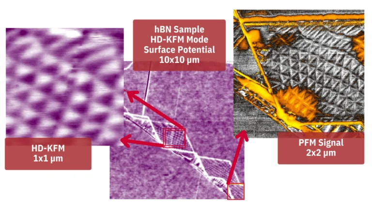
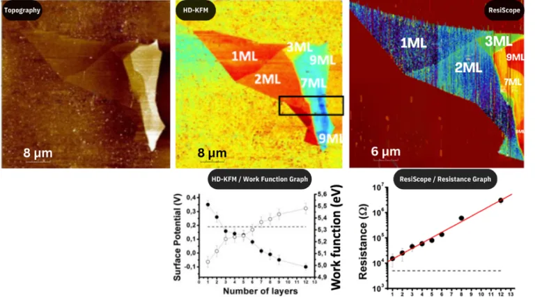
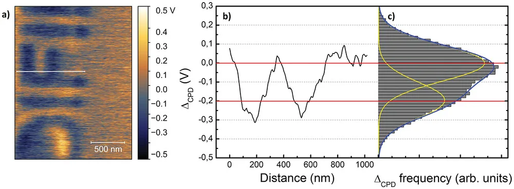
Operating in single-pass configuration with a Pt-coated conductive tip, the Nano-Observer’s HD-KFM (High-Definition Kelvin Force Microscopy) revealed nanoscale variations in surface potential. The contact potential difference (CPD) maps showed:
- Strong electrical contrast between MoS₂ nanopaths and SiO₂ substrate
- ~200 mV potential difference, corresponding to MoS₂ work function of 5.25 eV
- Spatial resolution in the tens of nanometers, limited only by tip radius and modulation voltage
- Histogram analysis clearly distinguishing the two material systems
ResiScope: Transport Properties at the Nanoscale
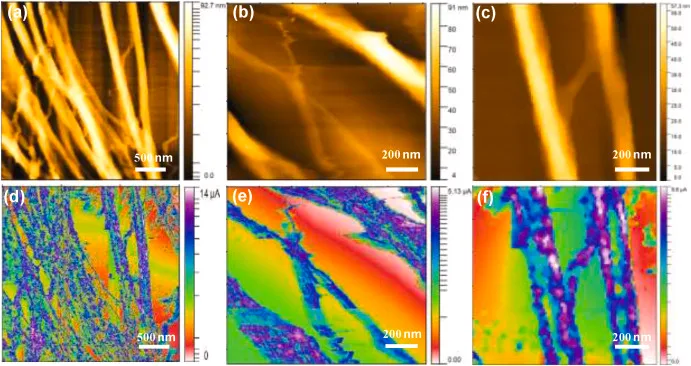
To probe the electrical transport properties, the team utilized the Nano-Observer’s ResiScope mode. This advanced conductive-AFM capability enables current and resistance mapping over wide dynamic ranges without damaging sensitive samples.
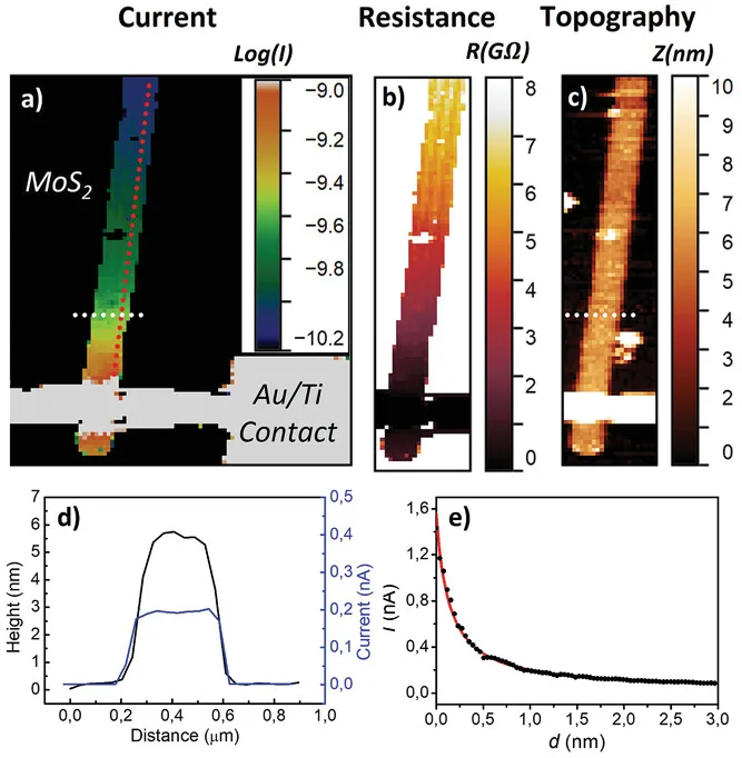
High-quality metallic nanocontacts were precisely aligned to MoS₂ nanofingers using t-SPL’s direct overlay capability. A p-doped single-crystal diamond tip then mapped current and resistance distributions under 0.5 V DC bias.
Key ResiScope Results:
- Strong electrical contrast at MoS₂-substrate edges
- Power-law decay of current: I(d) ∝ d⁻¹·¹ with distance from contact
- Local resistivity estimation: ~5 Ωm (competitive with state-of-the-art MoS₂)
- Real-time topography-correlated electrical maps
Why ResiScope for 2D Materials?
ResiScope’s key advantages for fragile 2D semiconductors:
- Wide Dynamic Range: Simultaneous measurement of high and low resistance regions
- Non-Destructive: Avoids sample or probe damage even on ultra-thin materials
- Quantitative: Direct resistance values, not just qualitative current maps
- Correlated Imaging: Real-time topography + electrical properties
Impact: Towards Scalable 2D Nanoelectronics
This work demonstrates a complete pathway from large-area growth to nanoscale electrical characterization of 2D semiconductor nanocircuits:
- Scalable Growth: cm²-scale uniform TMD films
- Non-Invasive Patterning: Additive t-SPL nanolithography
- Property Preservation: Clean 2H-semiconducting phase maintained
- Electrical Validation: Multi-modal nanoscopy confirms competitive transport
The Nano-Observer’s combination of HD-KFM and ResiScope provided essential nanoscale verification that these engineered nanocircuits retain the electronic properties needed for functional nanodevices.
As the field moves toward van der Waals heterostructures and integrated 2D nanoelectronics, this additive approach—validated by comprehensive electrical nanoscopy—opens new pathways for scalable manufacturing.
Reference: M. C. Giordano, G. Zambito, M. Gardella, F. Buatier de Mongeot, “Deterministic Thermal Sculpting of Large-Scale 2D Semiconductor Nanocircuits,” Adv. Mater. Interfaces, 2023, 10(5), 2201408. DOI: 10.1002/admi.202201408.