
Application fields
Key Features
EFM Mode
- High Sensitivity: Detect even the smallest variations in electric field gradients
- Excellent Spatial Resolution: Achieve lateral resolution down to a few nanometers
- Non-Destructive Imaging: Ideal for delicate or sensitive samples
- Quantitative Measurements: Map relative strengths of electric fields across surfaces
- Integration with Other Modes: Combine EFM with topography, mechanical, or other electrical modes for comprehensive analysis
EFM Mode
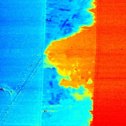
2 Nanotubes network deposited between 2 electrodes, EFM mode, 65µm scan
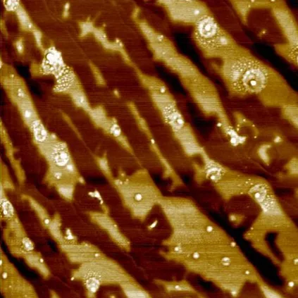
Graphene Scan Result with EFM 10 µm scan
- Superior Resolution: Our advanced EFM implementation offers unparalleled spatial resolution and sensitivity.
- User-Friendly Interface: Intuitive software makes EFM accessible to both experts and beginners.
- Versatility: Easily combine EFM with other AFM modes for comprehensive sample characterization.
- Cutting-Edge Research: Stay at the forefront of nanoscale electrical characterization with our continuously updated technology.
How does EFM work?
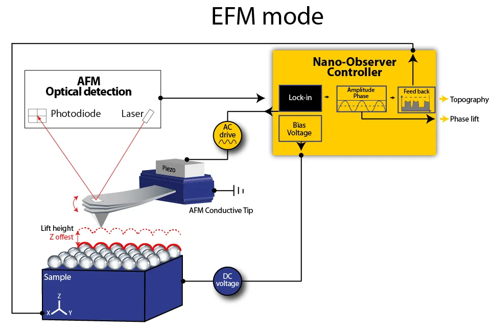
- Topography Scan: A metal-coated tip first scans the surface to record topography.
- Lift Mode: The tip is then raised to a specific height above the sample.
- Electric Field Detection: As the tip moves across the surface, it detects the gradient of electrical forces present.
- Data Recording: The system records the phase shifts of the cantilever oscillation, which correspond to the electric field gradient.
This two-pass technique allows for separate optimization of topographical and electrical measurements, ensuring high-quality data for both.
Specifications
- Lift Height Range: 5 nm – 100 nm (typical)
- Lateral Resolution: < 20 nm (tip-dependent)
- Compatible with all CSInstruments AFM systems
- Optional: Advanced EFM modules for quantitative measurements
Application Fields
Materials Science
- Characterization of dielectric thin films
- Study of charge distribution in composite materials
- Investigation of ferroelectric domain structures
Electronic Materials
- Failure analysis in microelectronic devices
- Detection and mapping of trapped charges
- Characterization of semiconductor dopant distributions
Life Sciences
- Study of charge distributions in biological membranes
- Investigation of electrical properties of biomaterials
Polymer Science
- Analysis of charge accumulation and dissipation in polymers
- Characterization of piezoelectric polymers
Nanotechnology
- Electrical characterization of nanomaterials (e.g., carbon nanotubes, graphene)
- Development and optimization of nanoelectronic devices
Questions about EFM Mode?
Ask the application scientists behind our AFMs and modes — about your samples, probes, set-up or which mode fits your measurement. We answer every message personally.