
Key takeaways
- HD-KFM™ distinguishes p- and n-doped regions of an SRAM device (30–50 mV between p-doped areas and n-doped channels, ~300 mV with the n-well) and reveals defective cells invisible in the topography.
- ResiScope™ on the same area, with the same cantilever, shows which of those cells conduct normally under 1 V bias.
- On a silicon dopant staircase, ResiScope follows resistance from ~100 Ω to ~1 MΩ across 500 nm steps in one scan.
- Soft ResiScope™ gives the same values without friction, and follows a VO₂ film from 25 to 50 °C as its current rises from ~100 pA to 6 nA.
Introduction
Electrical characterization at the scale of the device
Semiconductor devices are defined by doping, junctions and interfaces at the scale of tens of nanometres. Bulk electrical tests give the response of the whole device; electrical AFM modes map where it comes from. This note shows three complementary modes of the Nano-Observer II on memory devices, a dopant calibration structure and an oxide film: HD-KFM for surface potential, ResiScope for current and resistance, and Soft ResiScope for the same measurement without friction.
Techniques
HD-KFM and ResiScope
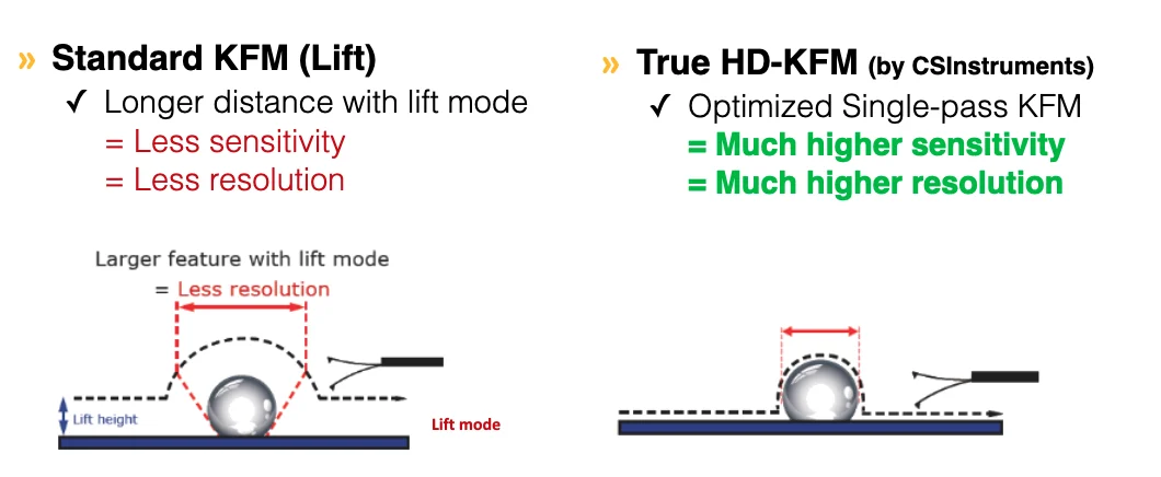
HD-KFM measures the surface potential without lift: the first eigenmode of the cantilever tracks the topography and the second, excited electrically, tracks the potential — closer to the surface, where the field is strongest (Figure 1). See single-pass vs lift-mode KPFM.
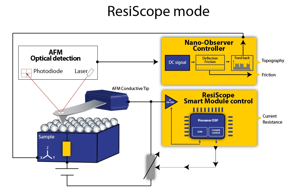
ResiScope is a contact mode that maps current and resistance over 10 orders of magnitude, from 50 fA (1 TΩ) to 1 mA (1 kΩ), without user intervention: a DSP selects the current-to-voltage amplifier in real time according to the resistance under the tip (Figure 2). A protective resistance limits the maximum current, minimizing local oxidation and cantilever self-heating. With a conventional fixed-range amplifier, insulating (pA) and conductive (µA–mA) regions of the same area cannot be measured at the same time.
Results
SRAM: surface potential and current on the same area
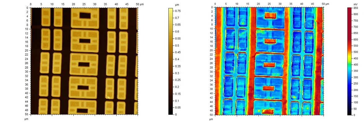
Figure 3 shows the topography and the HD-KFM surface potential of an SRAM device (50 µm). The potential differs by only 30–50 mV between p-doped areas and n-doped channels, and by about 300 mV with the n-well. Some cells show defects in the potential map that do not appear in the topography. Potential values relate to carrier concentration, but for quantitative values sMIM is better suited.
The same area was then measured in ResiScope without changing the set-up or the cantilever (Figure 4). Because the sample is biased (1 V), the current map also shows how the device performs: of the defects seen in Figure 3, one cell conducts normally while another shows no difference in current between p- and n-doped regions.
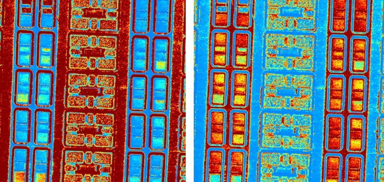
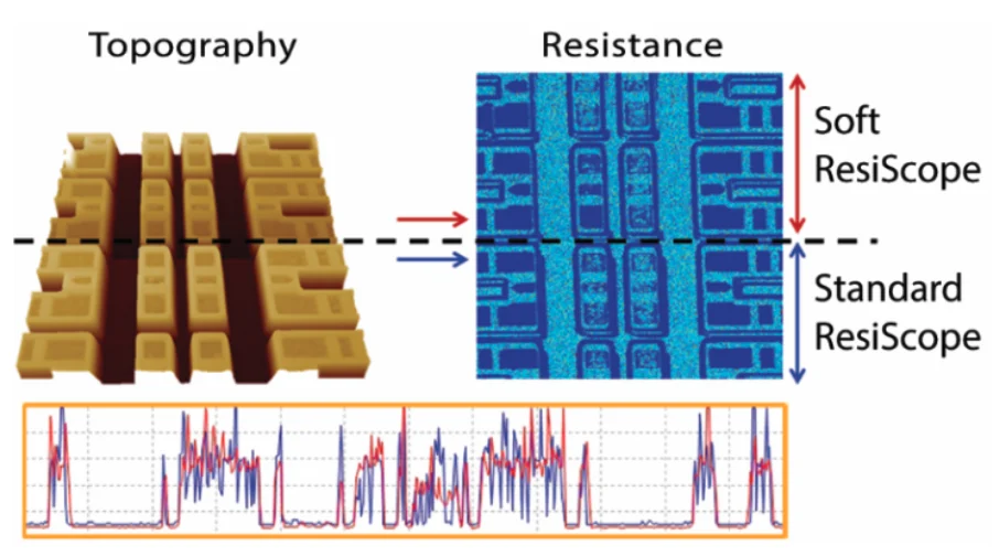
Soft ResiScope gives the same quantitative current and resistance as ResiScope, without the friction of contact scanning. In Figure 5 the top of the image was scanned in Soft ResiScope and the bottom in standard ResiScope: drain, source and channel show the same conductivity in both.
Results
Dopant profile on a silicon cross-section
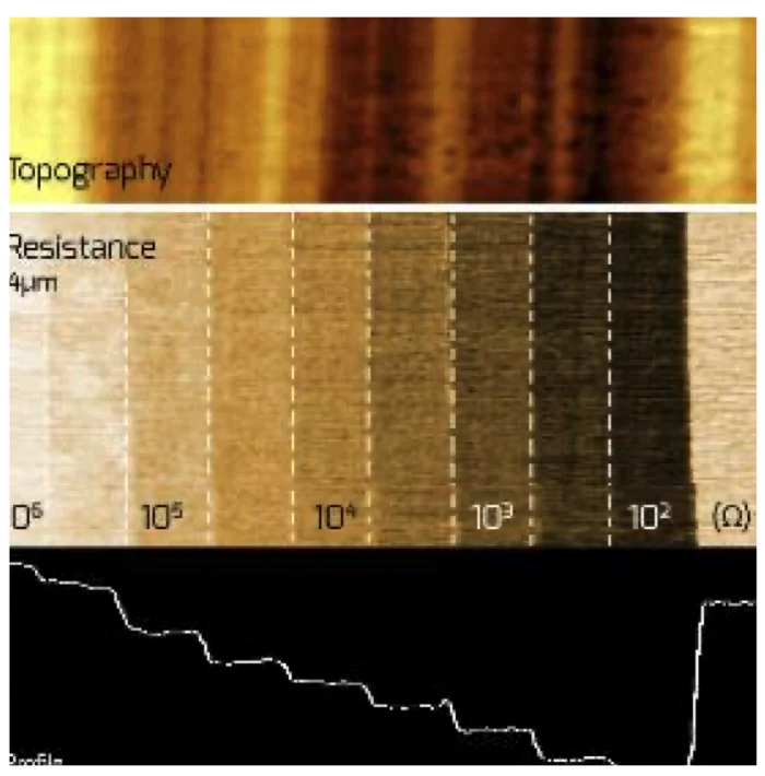
Figure 6 shows a cross-section of a silicon substrate with regions of increasing carrier implant (a staircase structure). Each region is 500 nm wide; the resistance decreases from about 1 MΩ to 100 Ω across the steps. ResiScope tracks these several orders of magnitude (10² to 10⁶ Ω) in real time, without losing sensitivity. Polishing lines are visible in the topography.
Results
VO₂: conductivity of grains during heating
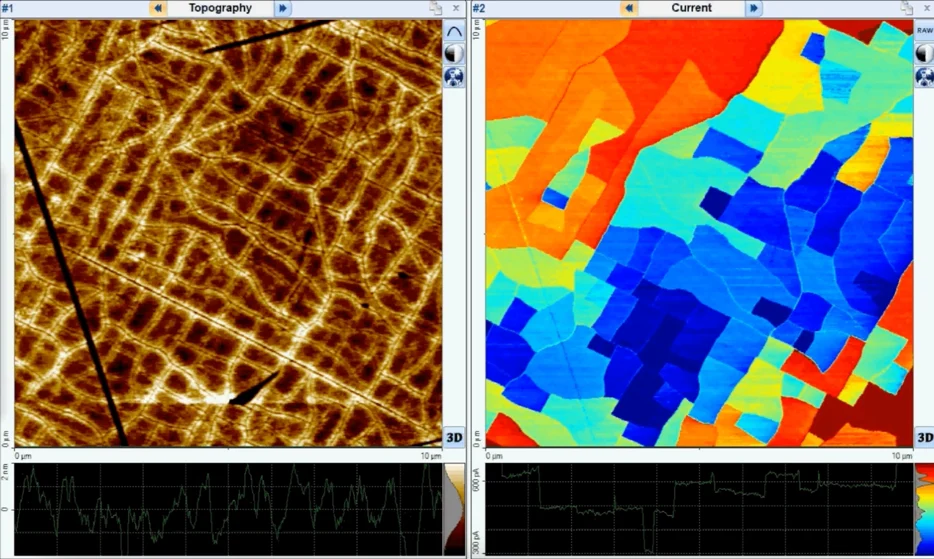
Vanadium dioxide (VO₂) has a semiconductor–metal transition near 68 °C, with large changes in electrical and optical properties. At room temperature (295 K), Soft ResiScope shows the grain structure in both topography and current (Figure 7): grain currents stay below 1 nA at 1 V bias and vary between about 300 and 650 pA from grain to grain.
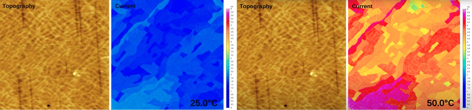
With the heating accessory, the sample was ramped from 25 to 50 °C at 0.1 °C/min (Figure 8). The position stays stable and the current of the VO₂ domains rises from about 100 pA to 6 nA. Because the amplifier gain is software-controlled, no set-up change is needed as the current grows by orders of magnitude, while variations of about 50 pA between grains remain visible.
Experimental
Measurement conditions
| Instrument | Nano-Observer II with HD-KFM, ResiScope and Soft ResiScope; heating accessory for the VO₂ ramp |
| SRAM | 50 µm scans; HD-KFM and ResiScope on the same area with the same cantilever; 1 V sample bias in ResiScope |
| Dopant staircase | Silicon cross-section, 500 nm wide implant regions, ResiScope |
| VO₂ | ANSCM-PT probe (Pt/Ir, AppNano); applied force 1.8 nN; lift between points 20 nm; 1 V bias; 295 K, then 25 → 50 °C at 0.1 °C/min |
Summary
Conclusion
HD-KFM maps surface potential with the resolution of the topography, revealing doped regions and defects; ResiScope and Soft ResiScope measure current and resistance over the largest dynamic range without changing the set-up, on insulating and highly conductive areas alike, and Soft ResiScope avoids friction. Because these modes are switched by software on the Nano-Observer II, the same area is measured with each — linking potential, conduction and device performance. They are also compatible with MFM and sMIM.
In this note
AFM modes used
FAQ
Frequently Asked Questions
How is AFM used to characterize semiconductor devices?
Electrical AFM modes map the properties that define a device at the nanoscale: surface potential with HD-KFM (doped regions, junctions, defects), current and resistance with ResiScope (device response under bias, dopant profiles), and permittivity and carrier concentration with sMIM.
Can AFM distinguish p- and n-doped regions?
Yes. On an SRAM device, HD-KFM showed differences of 30–50 mV between p-doped areas and n-doped channels and about 300 mV with the n-well, and revealed defective cells that were not visible in the topography.
Can ResiScope measure dopant profiles?
Yes. On a silicon cross-section with steps of increasing carrier implant, 500 nm wide each, ResiScope tracked resistances from about 100 Ω to 1 MΩ in real time, without changing the amplifier set-up.
Do HD-KFM and ResiScope require different set-ups?
No. On the Nano-Observer II the two modes are switched by software, with the same cantilever and without changing the set-up, so the same area is measured with both.
What is the advantage of Soft ResiScope on semiconductors?
It gives the same quantitative current and resistance as ResiScope, but without the friction of contact scanning, which limits damage. A scan of an SRAM measured half in Soft ResiScope and half in ResiScope showed the same results.
Can conductivity be followed during a temperature ramp?
Yes. With the heating accessory, Soft ResiScope followed the grains of a VO₂ film from 25 to 50 °C (0.1 °C/min); the current increased from about 100 pA to 6 nA with no amplifier change and stable position.
Characterize your semiconductor samples
Ask the application scientists behind our AFMs and modes — about your samples, probes, set-up or which mode fits your measurement. We answer every message personally.