
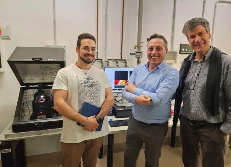
The lab
Nanostructured surfaces and 2D semiconductors
Prof. Francesco Buatier de Mongeot’s group in the Department of Physics of the University of Genoa makes nanostructured surfaces and thin films: 2D semiconductors such as MoS₂ shaped by thermal scanning probe lithography, flexible nanostripe electrodes for plasmonics, and superconducting films.
Their AFM
The group first worked with a Nano-Observer (first generation). On the same instrument it recorded the morphology of its samples in tapping mode, current maps with ResiScope and surface potential with HD-KFM, a KPFM mode that detects the potential on the second eigenmode of the cantilever (350 to 400 kHz), with low noise and sensitivity to structures below the surface. Four papers with these data have been published since 2020.
The lab has now moved to the Nano-Observer II, with ResiScope™ III for current and resistance over more than 10 decades and HD-KFM™ III for surface potential.
Result
Strain changes the work function of MoS₂
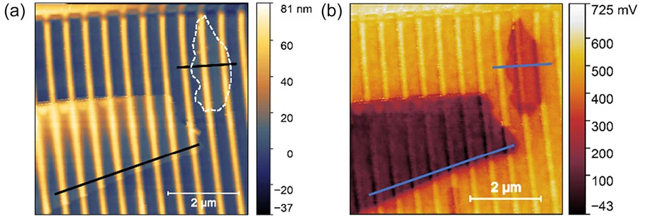
In the 2026 Small Science paper, a MoS₂ layer was transferred onto 3D nanoridges written by grayscale thermal scanning probe lithography. The ridges strain the layer locally, and the strain shifts its work function: this creates periodic lateral heterojunctions without a mask. HD-KFM (KPFM) on the Nano-Observer recorded topography and surface potential together, on the same area (Figure 1).
Publications
Papers with Nano-Observer data
Found by full-text search of the papers (OpenAlex); the measurement is taken from each paper’s methods.
- Strained 2D Semiconductor Lateral Heterojunctions via Grayscale Thermal-Scanning Probe LithographySmall Science, 2026HD-KFM (KPFM): topography and surface potential of strained MoS₂ on nanoridges.
- Deterministic Thermal Sculpting of Large-Scale 2D Semiconductor NanocircuitsAdvanced Materials Interfaces, 2022HD-KFM (KPFM) surface potential and ResiScope current maps of MoS₂ nanocircuits, on the same instrument.
- Impact of Annealing on TC and Structure of Titanium Thin FilmsIEEE Transactions on Applied Superconductivity, 2021Grain size of the superconducting titanium films.
- Large-area flexible nanostripe electrodes featuring plasmon hybridization engineeringNano Research, 2020Tapping-mode morphology and ResiScope conductive AFM of the nanostripe electrodes.
Your samples
Measure your own samples on the Nano-Observer II
Send a short description of the sample and what you need to measure. The application team recommends a mode and can run test measurements.