
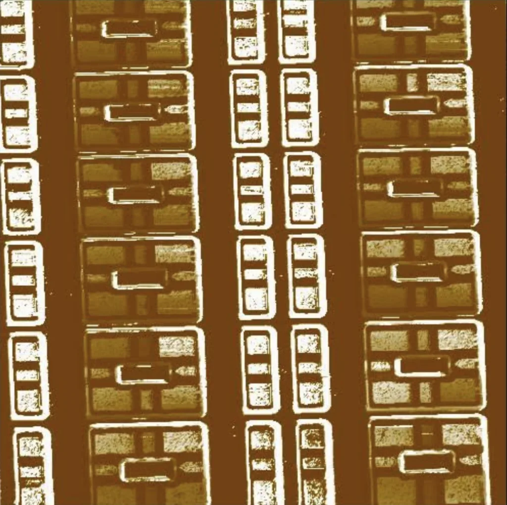
Application fields
Key Features
Conductive AFM
C-AFM mode offers:
- Wide Current Range: Measure currents from pA to µA
- High Spatial Resolution: Achieve lateral resolution down to a few nanometers
- Simultaneous Topography: Correlate electrical properties with surface features
- Spectroscopy Capabilities: Perform local I-V curve measurements
- Integration with Other Modes: Combine C-AFM with mechanical or thermal property mapping
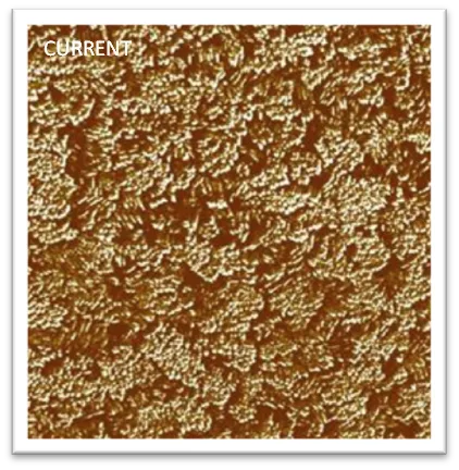
Benefits of conductive AFM on the Nano-Observer
- Superior Sensitivity: The C-AFM offers unparalleled current detection capabilities.
- User-Friendly Interface: Intuitive software makes C-AFM accessible to both experts and beginners.
- Versatility: Easily combine C-AFM with other AFM modes for comprehensive sample characterization.
- Expert Support: Our team of specialists provides ongoing support and training.
- Cutting-Edge Research: Stay at the forefront of nanoscale electrical characterization with our continuously updated technology.
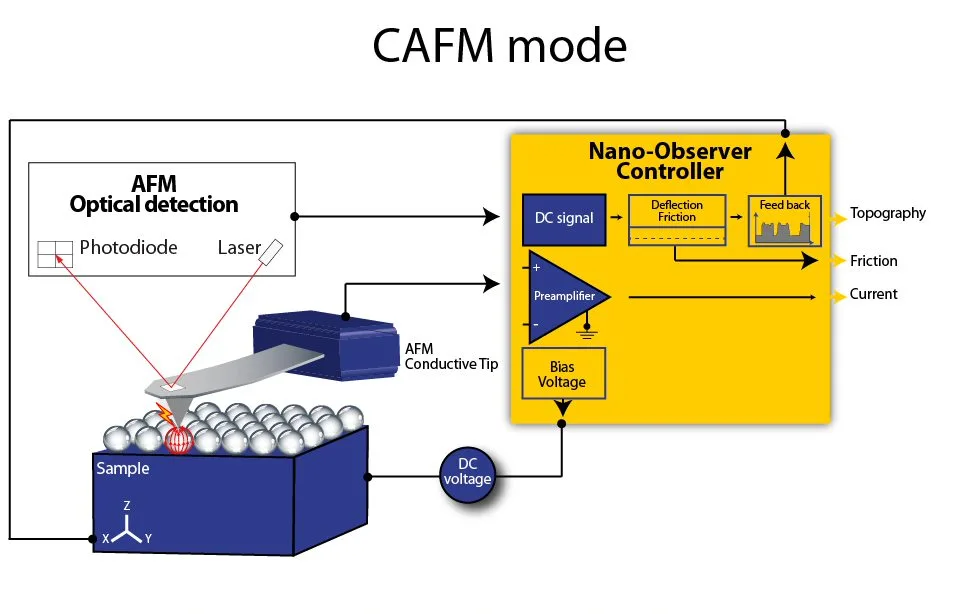
How does Conductive AFM work?
C-AFM operates by scanning a conductive AFM tip across the sample surface while applying a bias voltage. The resulting current flow is measured, allowing for:
- High-resolution mapping of current distribution
- Quantitative measurements of local conductivity
- Identification of conductive pathways and defects
Application Fields
Application fields
Semiconductor Research
- Characterization of dopant distributions
- Analysis of thin film solar cells
- Investigation of nanoelectronic devices
Materials Science
- Study of conductive polymers and composites
- Examination of corrosion processes
- Analysis of battery electrode materials
Nanotechnology
- Characterization of carbon nanotubes and graphene
- Development of nanoscale sensors and actuator
Energy Research
- Optimization of photovoltaic materials
- Investigation of fuel cell components
- Study of energy storage materials
Biology and Medicine
- Analysis of conductive biomaterials
- Investigation of cellular electrical properties
- Development of biosensors
The limit of conventional C-AFM
When one current range is not enough: ResiScope™
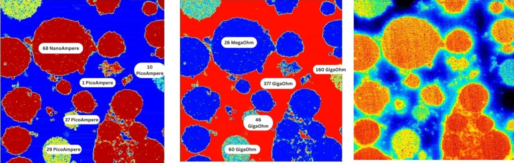
Conventional conductive AFM measures the current with one amplifier whose gain is fixed before the scan, so only about four decades are read correctly. Highly conductive areas saturate the amplifier — often around 10 nA — while insulating areas disappear in the noise. On heterogeneous samples such as battery electrodes, solar cells, composites or 2D materials the image is only partly quantitative, and capacitive effects and surface charging add artefacts.
ResiScope™ is CSInstruments’ answer. It works like C-AFM — a conductive tip, a bias voltage, contact with the sample — but a DSP-controlled amplifier re-chooses its gain at every measured point. Resistance from 10² to 10¹² Ω and current from fA to µA are measured in the same scan, together with the topography, with no saturation, no manual range switching and real-time current protection for tip and sample.
- 10 decades in one scan — 10²–10¹² Ω and fA to µA, where standard C-AFM covers about four.
- No clipped domains, no charging baseline — conductive and insulating areas are both quantitative.
- Fragile samples — Soft ResiScope™ measures in intermittent contact, without shear.
- Surface potential on the same area — combine with HD-KFM™, single-pass Kelvin probe force microscopy (KPFM), to correlate conductivity and work function.
- Where — ResiScope™ III on the Nano-Observer II, ResiScope™ II on the Nano-Observer One Plus, and on existing AFMs with the Galaxy Dual Controller.
Advanced electrical characterization
Beyond C-AFM.
Meet ResiScope™.
Standard conductive AFM measures current — and stops there. ResiScope™ delivers simultaneous, quantitative resistance and current mapping across 10 full decades, in a single pass, without damaging your sample.
10 dec.
Dynamic range
10² to 10¹² Ω — conductive and insulating regions in one scan.
fA–µA
Current sensitivity
Femtoampere detection — signals invisible to conventional C-AFM.
1× pass
Single acquisition
Resistance, current, and topography — captured simultaneously.
Ideal applications
See it in action
Real measurements on real samples — how ResiScope™ performs where C-AFM falls short.
Energy Materials
Battery Electrode Characterization
10-decade range captures pA binder phases and µA active domains in one pass.
Read note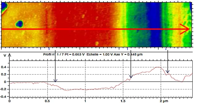
Photovoltaics
KPFM on Perovskite Solar Cells
Grain boundary potentials resolved at sub-10 nm with HD-KFM III and ResiScope™.
Read note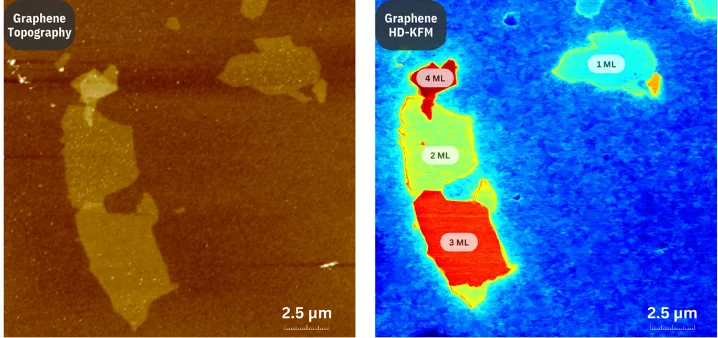
2D Materials
HD-KFM for Graphene, hBN & MoS₂
Moiré superlattices and layer-by-layer work function mapping across 10 decades.
Read noteFAQ
Frequently Asked Questions
What is Conductive AFM (C-AFM) and what does it measure?
Conductive AFM (C-AFM) is an AFM technique that simultaneously maps surface topography and local electrical current at the nanoscale. A conductive tip in contact with the sample measures current flow as a function of position, revealing spatial variations in conductivity, resistance, and charge transport at nanometer-scale resolution.
What are the limitations of standard C-AFM?
Standard C-AFM measures current only — resistance must be inferred indirectly, which introduces significant inaccuracy. Its dynamic range is typically limited to a few decades (nA to µA), meaning highly resistive regions saturate or disappear from the map. High contact forces required to maintain current flow also risk damaging soft or fragile samples such as battery materials, 2D materials, or organic films.
How does ResiScope™ differ from standard C-AFM?
ResiScope™ goes beyond C-AFM in three fundamental ways. First, it measures resistance directly and quantitatively at every pixel — not just current. Second, its 10-decade dynamic range (10² to 10¹² Ω, fA to µA) covers both conductive and insulating regions in a single scan without saturation. Third, its Soft-ResiScope mode enables measurements at very low contact forces, preserving fragile samples that standard C-AFM would damage.
Can ResiScope™ replace C-AFM entirely?
Yes — ResiScope™ is a direct upgrade to standard C-AFM. It performs everything C-AFM does, and adds direct resistance mapping, 10× wider dynamic range, real-time auto-gain control, and soft-mode operation. Researchers who switch from C-AFM to ResiScope™ gain quantitative resistance data and full dynamic range without changing their workflow.
What is the dynamic range of ResiScope™ compared to other C-AFM systems?
ResiScope™ covers 10 full decades of resistance — from 10² to 10¹² Ω — and detects currents from femtoamperes (fA) to microamperes (µA) in a single pass. Standard C-AFM systems typically cover 4–5 decades and require manual gain switching or multiple scans. ResiScope™'s real-time DSP auto-gain system handles the full range automatically.
Which materials and applications is ResiScope™ best suited for?
ResiScope™ is optimized for solid-state batteries (mapping both conductive active particles and resistive binders/electrolytes), semiconductors and nanoelectronics (failure analysis, leakage current), 2D materials (graphene, MoS₂, hBN), photovoltaic cells (grain boundary analysis, defect mapping), organic electronics, thin films, and polymers. Any application requiring electrical characterization across a wide conductivity range benefits from ResiScope™'s 10-decade range.
What is Soft-ResiScope and when should I use it?
Soft-ResiScope combines ResiScope™ electrical measurements with Soft-IC mode — a friction-free, constant-force approach where the tip approaches, holds, measures, then retracts at each pixel without lateral contact. This eliminates friction-induced artifacts and sample damage, making it ideal for battery separators, solid electrolytes, organic films, 2D materials, and any soft or layered sample where standard contact-mode scanning would deform or destroy the surface.
How does ResiScope™ compare to SSRM?
SSRM operates in a narrow resistance range (typically up to 10⁶–10⁷ Ω), requires high contact forces that damage soft materials, and measures current only. ResiScope™ measures resistance directly from 10² to 10¹² Ω, operates at low forces with Soft-ResiScope, and delivers quantitative resistance values at every pixel. For battery materials and heterogeneous samples, ResiScope™ provides complete characterization in a single scan where SSRM would require multiple setups.
Is ResiScope™ available for existing AFM systems?
Yes. ResiScope™ is available as a native mode on CSI's Nano-Observer II and Nano-Observer One Plus standalone AFMs, and as an upgrade for existing third-party AFM systems via the Galaxy Dual Controller — compatible with Bruker Multimode/Dimension, Keysight/Agilent 5500/5100/54x0/5600, and other legacy platforms.
What AFM has the best C-AFM performance?
For researchers requiring the widest dynamic range, direct quantitative resistance mapping, and non-destructive measurements on sensitive samples, ResiScope™ on CSI's Nano-Observer II or Nano-Observer One Plus is the most capable solution available. Unlike competing C-AFM implementations limited to 4–5 decades, ResiScope™ covers 10 full decades of resistance in a single pass, with femtoampere sensitivity and real-time auto-gain — simultaneously providing topography, current, and direct resistance maps without saturation or gain switching.
Why does the current saturate in conductive AFM?
A conventional C-AFM amplifier has one gain, chosen before the scan, covering roughly four decades. Areas more conductive than that range clip at the amplifier limit (often around 10 nA) and areas below it are lost in the noise. ResiScope avoids this by re-choosing the gain at every measured point, over 10 decades.
Can current and surface potential be measured on the same area?
Yes. On the Nano-Observer II, ResiScope (current and resistance) and HD-KFM (single-pass KPFM surface potential) can be run on the same area without moving the sample, to correlate conductivity with work function.
Questions about C-AFM?
Ask the application scientists behind our AFMs and modes — about your samples, probes, set-up or which mode fits your measurement. We answer every message personally.