
What do you need to measure?
Start from the measurement
Surface potential
KPFM, in one pass
HD-KFM™ uses the second eigenmode of the cantilever, so topography and surface potential come out of the same line. There is no lift pass and no topographic crosstalk of the kind lift-mode KPFM picks up.
- Work function contrast that separates graphene from one to four layers
- Moiré domains in folded hBN, seen in the potential channel
- The same tip then switches to ResiScope, on the same area
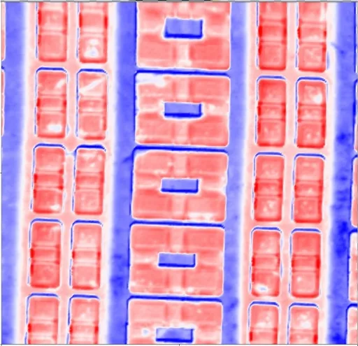
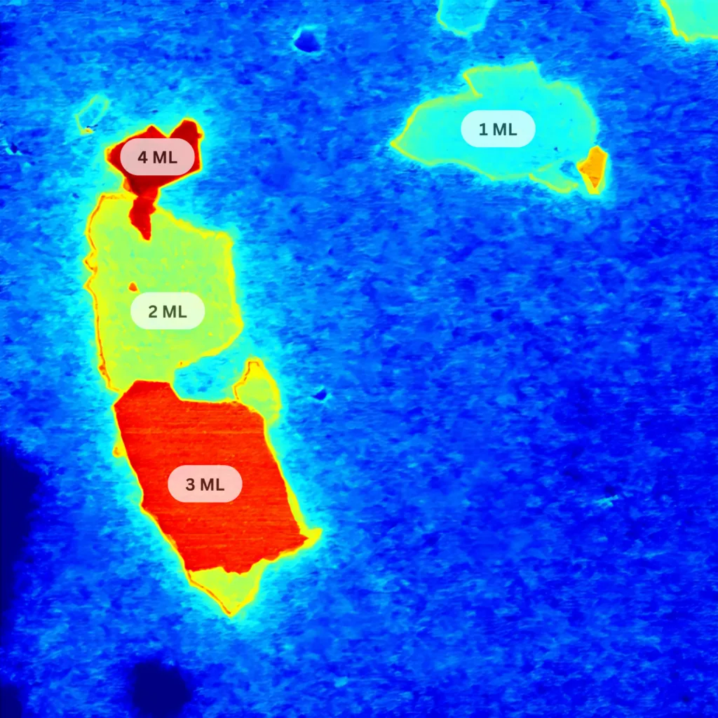
Graphene, layer by layer
HD-KFM surface potential, 20 µm. The work function changes with the number of layers.
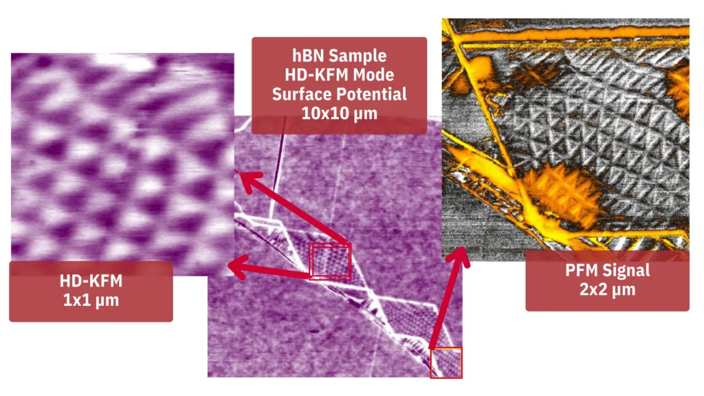
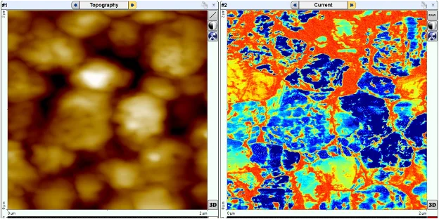
Perovskite solar cell
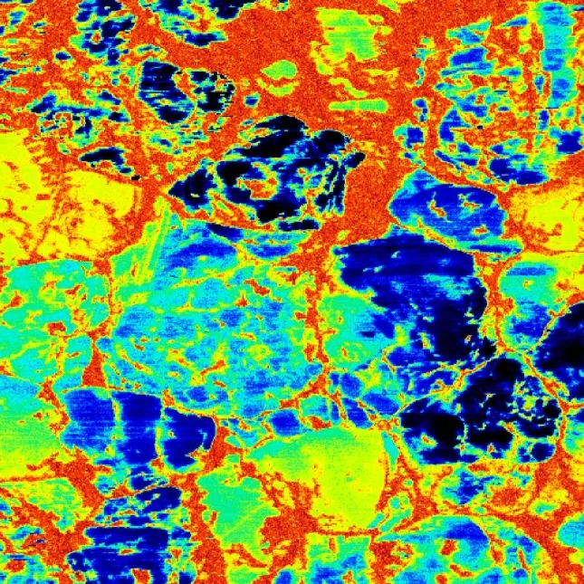
Surface potential across the grains, where the cell actually gains and loses performance.
Resistance and current
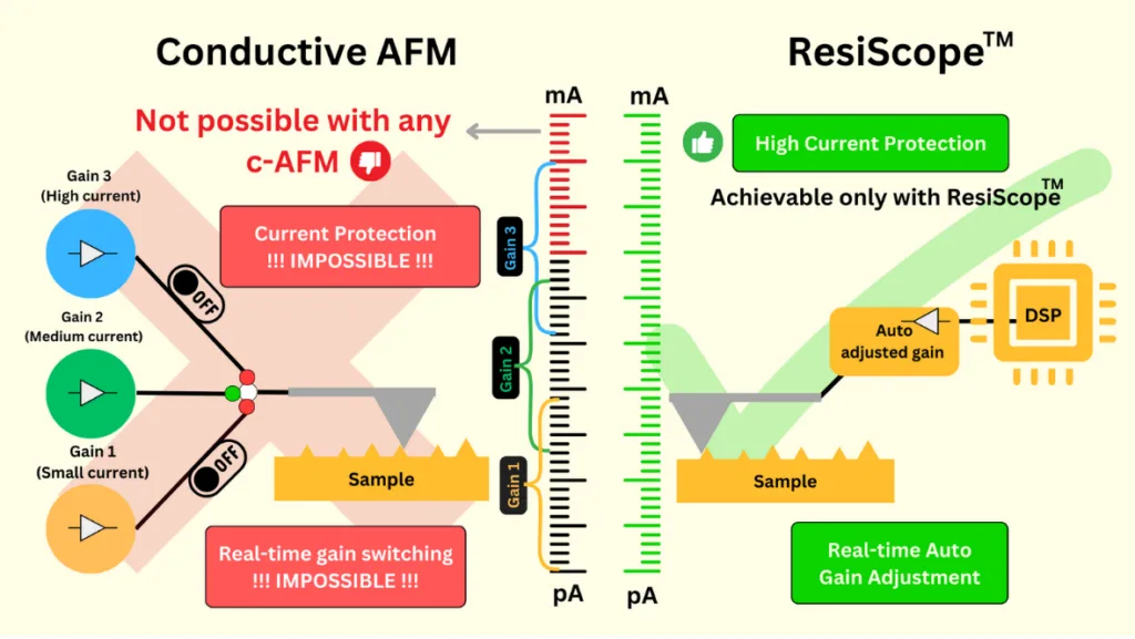
Conductive AFM that does not saturate
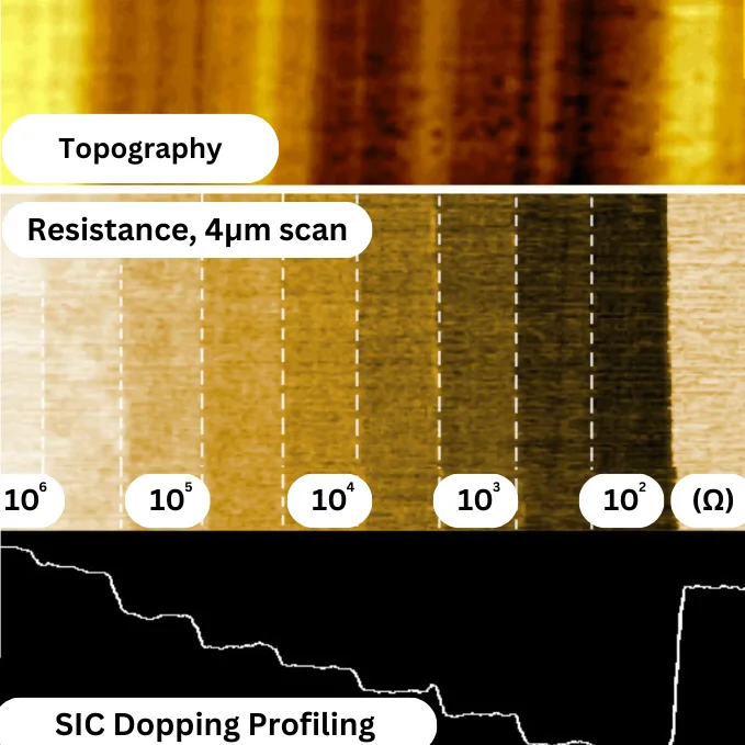
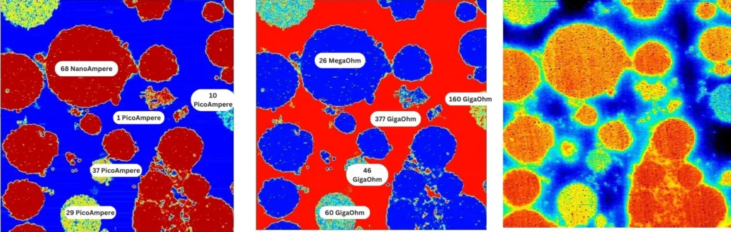
A conductive-AFM amplifier covers a slice of the current range and clips everything outside it. ResiScope™ III follows the sample across ten decades, so an insulating domain and a conducting path in the same scan both stay measurable.
- 10² to 10¹² Ω in one scan, no manual range switching
- Current and resistance together with the topography
- The same measurement on polymers and battery electrodes, in Soft ResiScope
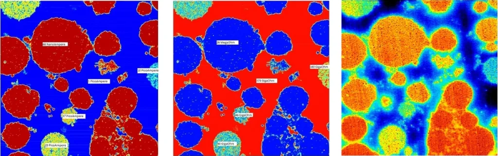
Battery electrode
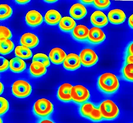
Soft ResiScope, 50 µm. Conductivity mapped without dragging the tip across the electrode.
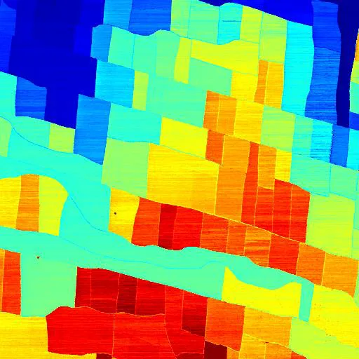
Fragile samples
Electrical data without scratching the sample
Soft Interaction Control touches the surface once per point, measures, and lifts clear before moving on. There is no lateral force, so polymers, organic layers and loosely bound particles survive the scan — and the electrical channels still run.
- Soft ResiScope for resistance on soft electrodes
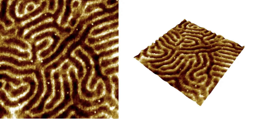
- Soft PFM and Soft SThM on the same intermittent contact
- Stiffness and adhesion from the same force curve, with Soft MEKA
From the lab
Scan results by application
A few of the measurements already on the site. Each card opens the full gallery.
Read the measurement
Application notes
New AFM, or the one you have
Two ways to run these modes
Searching for a Bruker, Park, Asylum or Nanosurf system? If the head you already own still works, the usual path is a controller upgrade rather than a new microscope.
FAQ
Frequently Asked Questions
What is the difference between KPFM and HD-KFM?
Standard KPFM often maps surface potential on a second pass, lifted above the topography line, so the potential is averaged and can pick up topographic artifacts. HD-KFM records topography and surface potential together, in one pass, using the second eigenmode of the cantilever. On graphene it separates one to four layers by their work function.
How is ResiScope different from conductive AFM?
Conductive AFM measures current and saturates when the sample spans a wide resistance range. ResiScope™ III covers 10² to 10¹² Ω in a single scan, so an insulating region and a conducting region of the same sample both stay in range.
Can HD-KFM and ResiScope be added to an existing AFM?
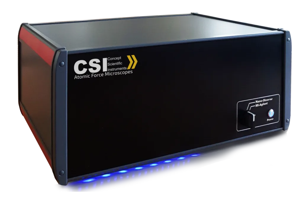
Yes. The Galaxy Dual Controller upgrades Bruker MultiMode and Dimension 3000/3100 AFMs, and Molecular Imaging, Agilent and Keysight 5100, 5400/5420, 5500, 5600LS and PicoSPM systems. It keeps the AFM’s existing modes and adds HD-KFM, ResiScope and Soft Interaction Control.
How much does an electrical AFM cost?
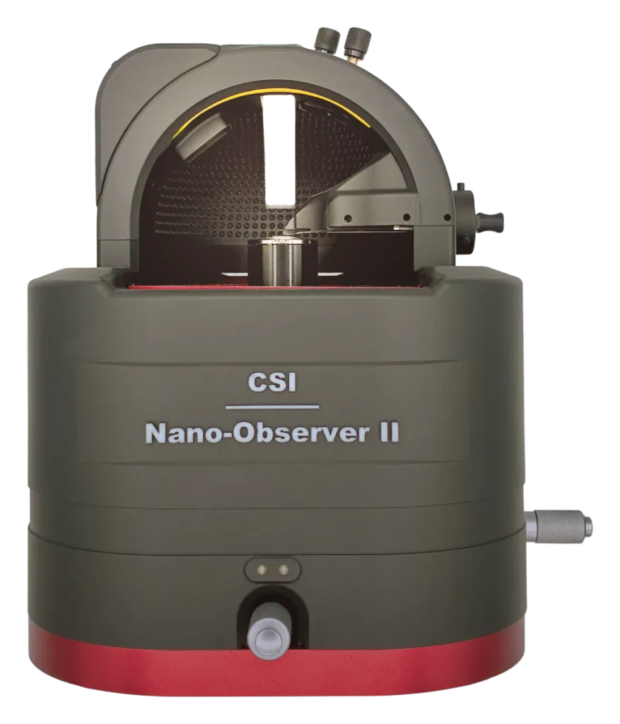
There is no public price list: the quotation depends on whether you need a Nano-Observer II or a controller upgrade, and on which modes you add. Send the measurement you need and the team replies with a quotation.
Can CSInstruments measure my sample before I buy?
Yes. Send a short description of the material and the measurement — surface potential, resistance, or both — and the application team recommends a mode and can run test scans.
Request a quote
Tell us the measurement — surface potential, resistance, or both — and the material. If you already have an AFM, name the model. We reply with the mode and the system that fits.