
Single pass
Topography and surface potential, at the same time
One tip, one trajectory, one pass — both channels come out together.
- Single pass — no lift, no second line
- 2nd eigenmode harmonic detection
- Tip stays 0.1–0.5 nm from the surface
- Potential contrast at the resolution of the topography
- Noise level below 1 mV
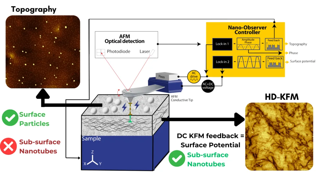
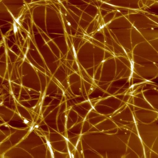
- Sub-surface detection — structures buried under the surface (e.g. nanotubes in a polymer)
At a glance
HD-KFM™ III in numbers
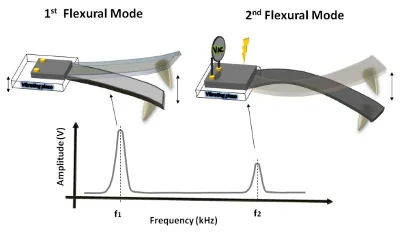
Bimodal dual-frequency excitation: the first flexural mode follows the topography while the second, electrically excited mode measures the surface potential — amplified by the Q factor of that mode.
What sets HD-KFM™ apart
The second eigenmode: potential measured at its own resonance
HD-KFM™ is bimodal: one cantilever, two resonances. Instead of reading the potential in a second pass or as a low-frequency sideband, it drives the cantilever’s second eigenmode electrically — so topography and surface potential are recorded together, with the tip 0.1–0.5 nm from the surface.
- f1 · Sideband KFM (≈15 kHz)The low frequency at which sideband KFM reads the electrical signal.
- f2 · Mechanical resonance (≈70 kHz)The first flexural mode of the cantilever follows the topography.
- f3 · HD-KFM™ second eigenmode (≈400 kHz)Excited electrically (VAC) to measure the surface potential — a signal amplified by the Q factor of that mode, far from the topography frequency, in the same single pass.
Key Features
HD-KFM III
HD-KFM III: Harmonic Detection – Kelvin Probe Force Microscopy
HD-KFM III is an advanced Kelvin Probe Force Microscopy solution that builds upon previous generations with several key improvements. Here are its notable features and capabilities:
- Enhanced Measurement Accuracy: The system offers improved accuracy and significantly reduced background noise compared to previous versions, enabling more precise surface potential measurements at the nanoscale.
- Simultaneous Multi-Parameter Imaging: One of the most impressive capabilities is the ability to perform simultaneous MFM (Magnetic Force Microscopy) and HD-KFM measurements, allowing researchers to correlate magnetic and electrical properties in a single scan.
- Advanced Dielectric Capabilities: The system includes dC/dZ functionality, making it particularly valuable for dielectric measurements and characterization of insulating materials.
- Electrical Field Compensation: Features an MFM with EFC (Electrical Field Compensation) option, which helps eliminate electrical interference during magnetic measurements.
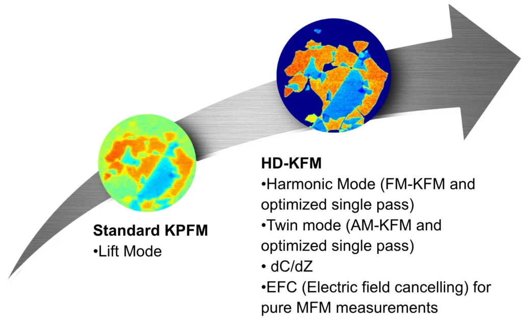
This technology represents a significant advancement in surface characterization capabilities, particularly valuable for research in materials science, semiconductor analysis, and advanced electronic materials development.
Advanced features
dC/dZ and EFC
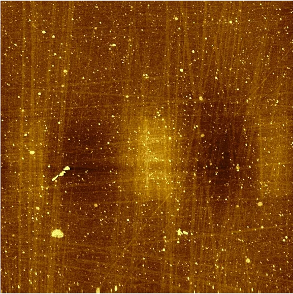
dC/dZ Measurements: dC/dZ measures the change in capacitance with respect to the tip-sample distance, providing information about local dielectric properties.
Benefits: Enables mapping of dielectric constants and investigation of thin film properties at the nanoscale.
EFC (Electrical Field Compensation for MFM):
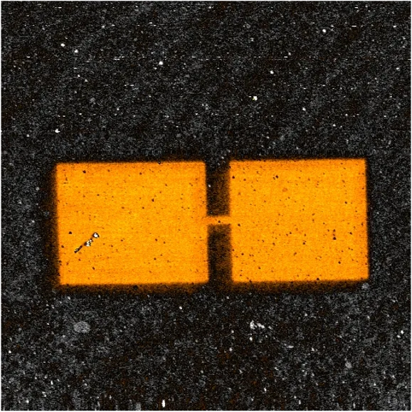
EFC nullifies the electrostatic interaction between the tip and sample during Magnetic Force Microscopy measurements.
Benefits: Allows for pure magnetic measurements without electrostatic interference, crucial for accurate characterization of magnetic nanostructures.
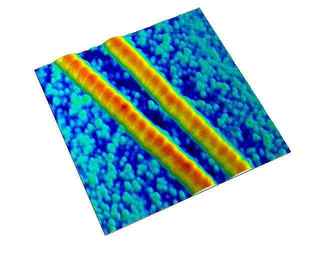
Sub-surface nanotubes in a polymer, seen by HD-KFM
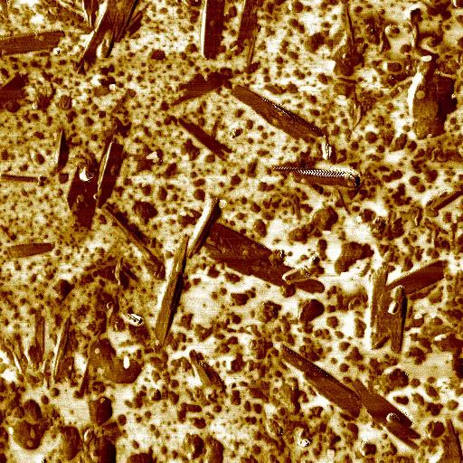
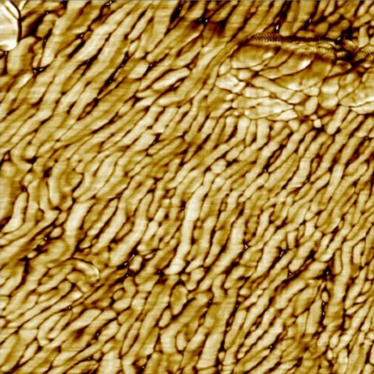
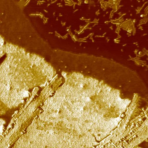
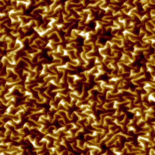
Gallery
Energy
Polymers
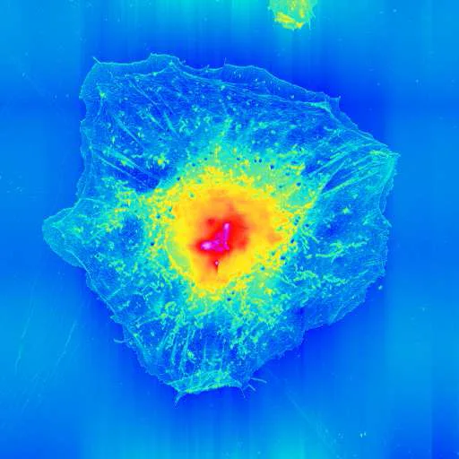
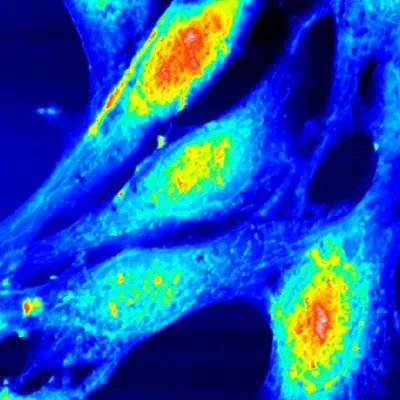
Biological Samples
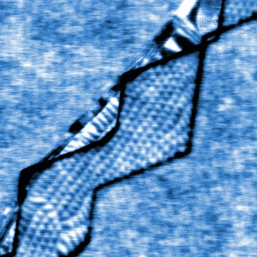
2D Materials
Semiconductors
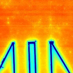
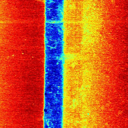
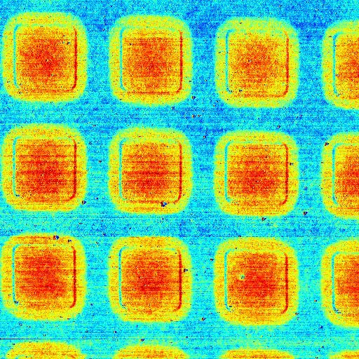
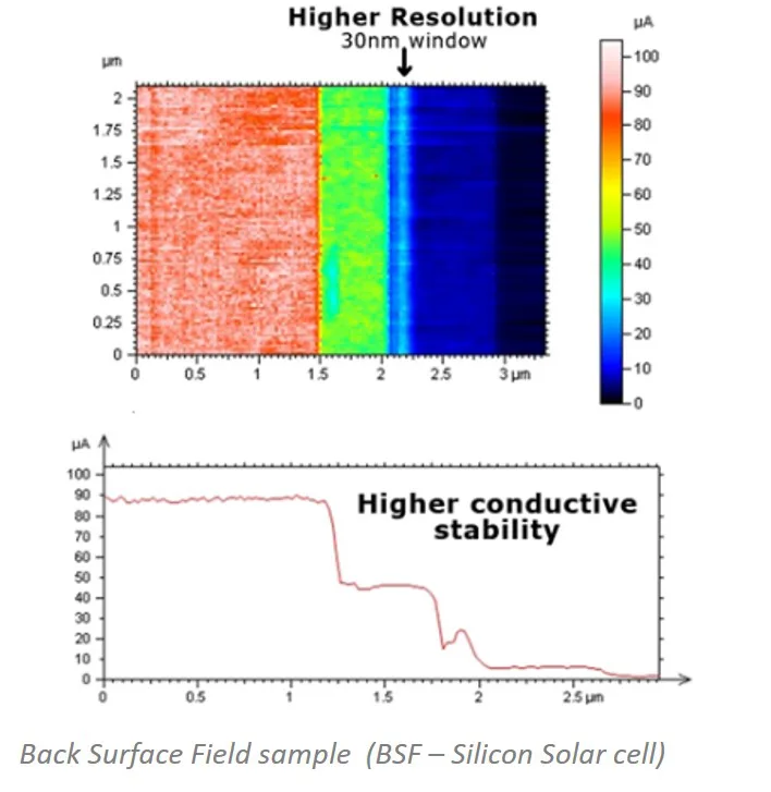
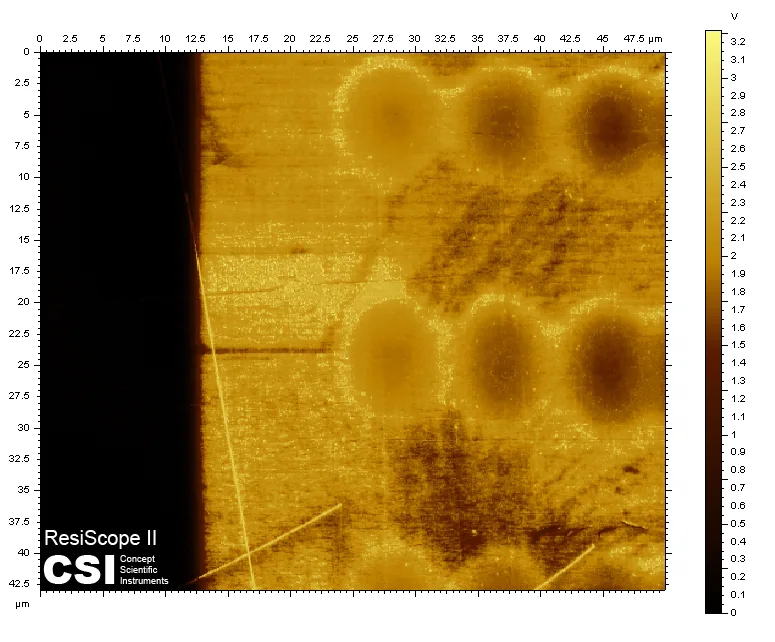
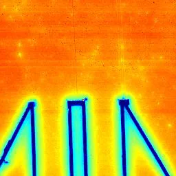
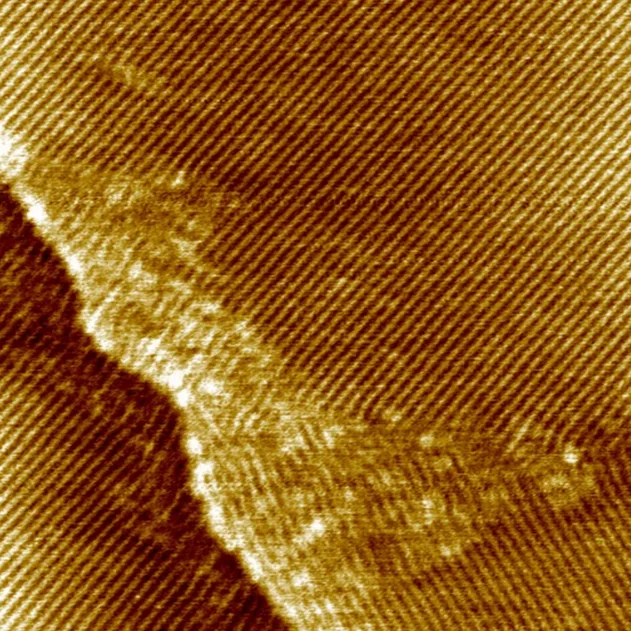
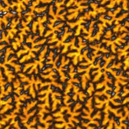
Materials Science
Principle of HD-KFM III
Bimodal Dual Frequency Excitation
Topography Frequency:
- The first flexural mode of the cantilever is excited mechanically.
- This frequency is used to measure and control the sample topography.
- Allows for precise tracking of surface features without interference
Surface Potential Frequency:
- The second flexural mode of the cantilever is excited electrically.
- This separate frequency is dedicated to measuring surface potential.
- Enables simultaneous, independent measurement of topography and surface
Signal Amplification:
- The use of the second eigenmode for electrical excitation inherently amplifies the signal.
- This amplification occurs even with very small applied AC voltages.
- Results in improved signal-to-noise ratio and higher sensitivity to small potential differences.
Enhanced Signal Amplification:
- The VAC bias is fine-tuned to the second eigenmode of the cantilever.
- This tuning amplifies the signal by the Q factor of the second mode.
- The Q factor amplification can be significant, often 100 times or more, greatly enhancing sensitivity.
Single-Pass Operation
Single-pass operation in HD-KFM III represents a significant advancement over traditional Kelvin Probe Force Microscopy techniques:
Elimination of Lift Scans:
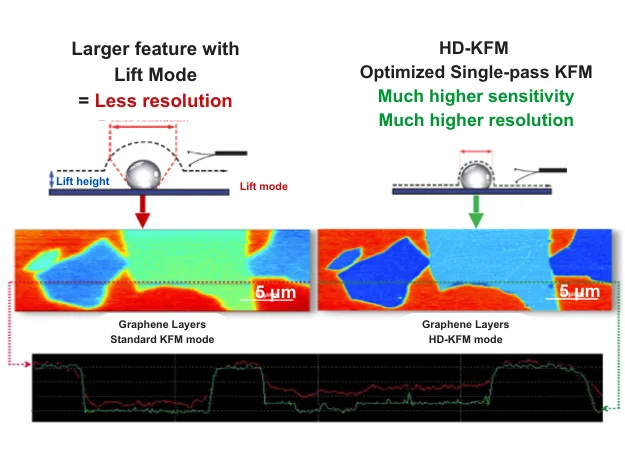
- Traditional KFM requires two passes: one for topography and another lifted pass for potential measurement.
- HD-KFM III combines both measurements in a single pass, saving time and reducing potential errors.
Proximity to Surface:
- The tip operates at a typical minimum distance of 0.1-0.5 nm from the sample surface.
- This close proximity allows for much stronger interaction with the sample’s electrostatic field.
- Compared to standard KFM (10-100 nm lift height), HD-KFM III probes an electrostatic field 100-10,000 times stronger.
Enhanced Resolution and Sensitivity:
- Closer proximity leads to significant improvements in lateral resolution.
- Sensitivity is greatly enhanced, allowing for detection of subtle variations in surface potential.
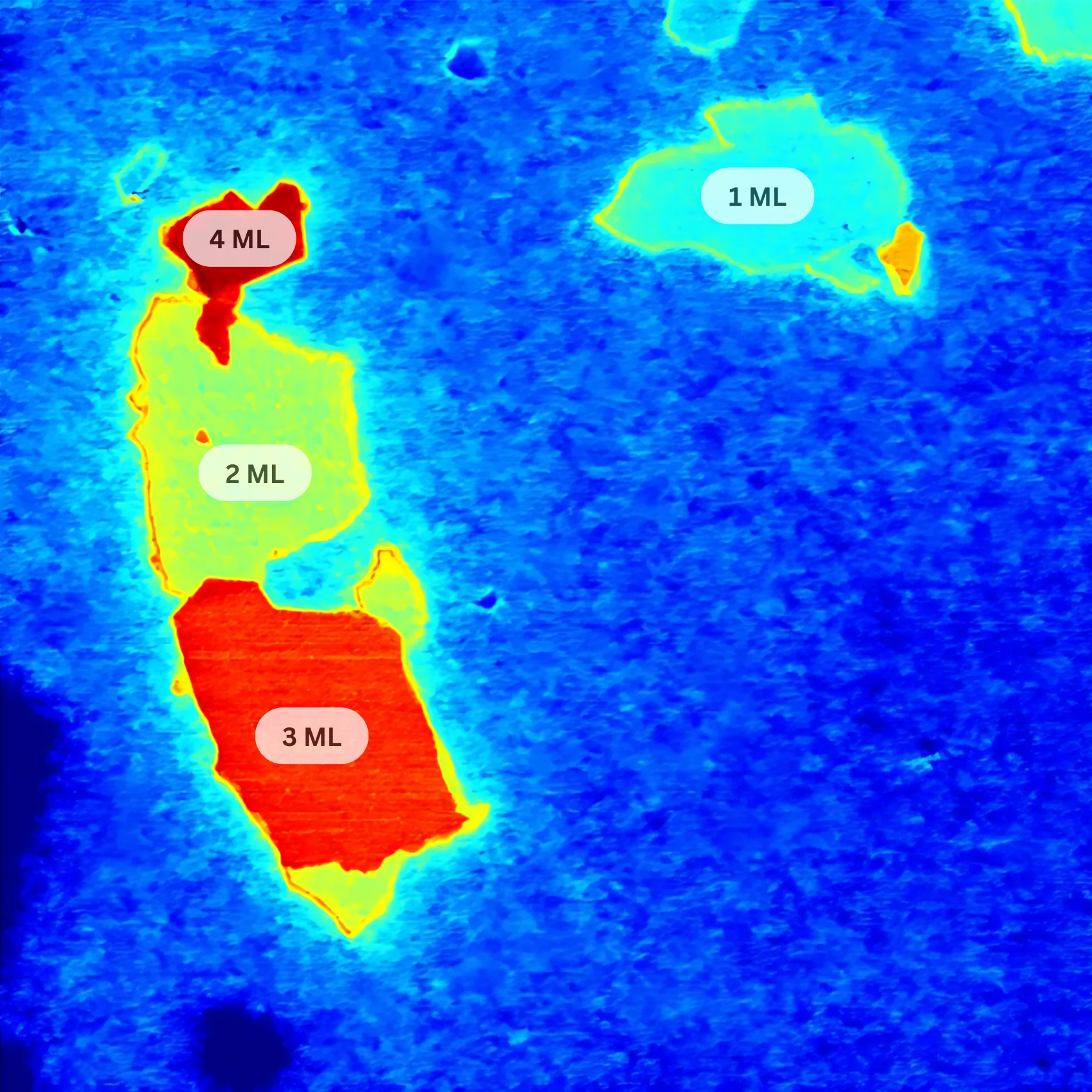
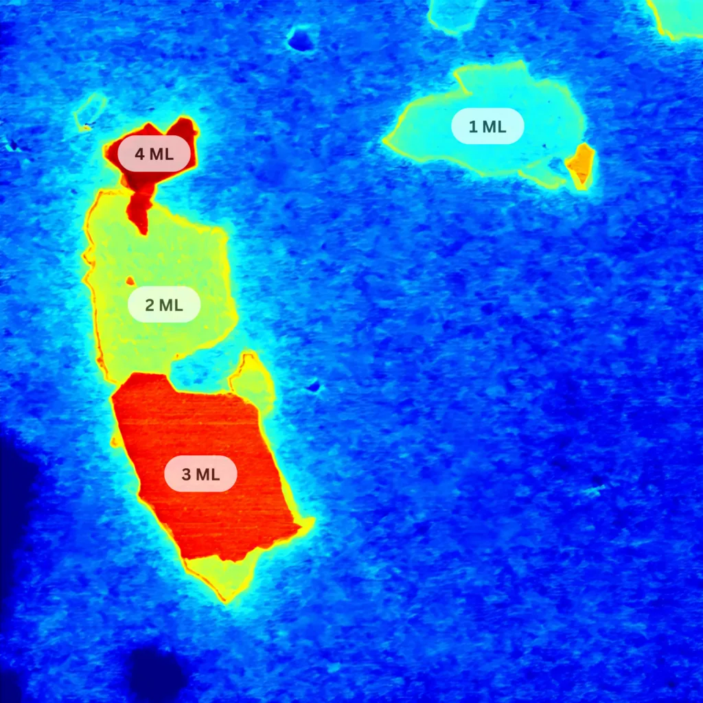
- Enables clear differentiation between features like single and multiple layers of 2D materials.
Improved Stability:
- The second eigenmode has a stiffer effective spring constant compared to the fundamental mode.
- This increased stiffness provides more stable oscillation during surface scanning.
- Stability translates to more reliable and consistent measurements, especially on challenging samples.
Automated Frequency Optimization:
- The Vac bias is fine-tuned to the Second eigenmode automatically by the software without user intervention.
- Patented algorithm selects the best frequency position around the resonance peak.
- Achieves better resolution and sensitivity through optimized frequency selection.
Standard KFM vs HD-KFM
Specifications
HD-KFM III Technical Specifications
- Operating Mode: Single-pass
- Tip-Sample Distance: 0.1 – 0.5 nm (typical)
- Excitation Modes: Dual-frequency (Bimodal)
- Topography Measurement: First flexural mode frequency (mechanical excitation)
- Surface Potential Measurement: Second flexural mode frequency (electrical excitation)
- Signal Amplification: Q factor enhancement in the second eigenmode
- VAC Bias: Optimized for second eigenmode, enabling lower voltage applications
- Feedback System: Dual feedback control (topography and electrical signals)
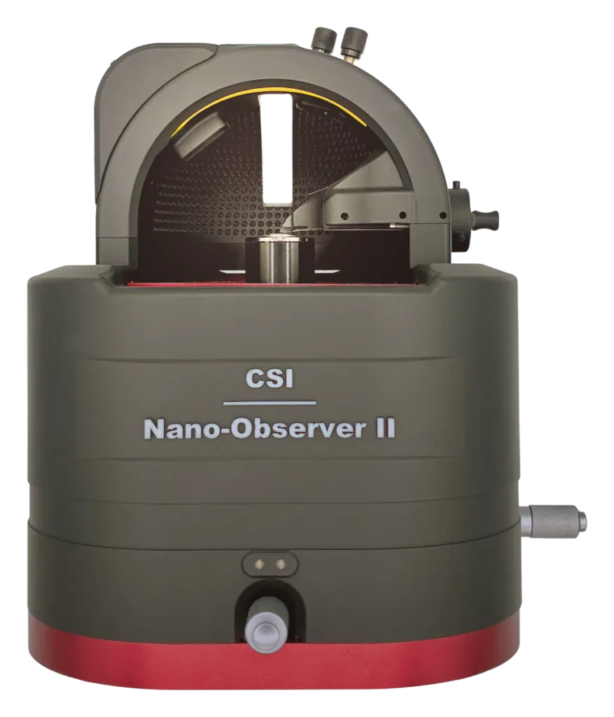
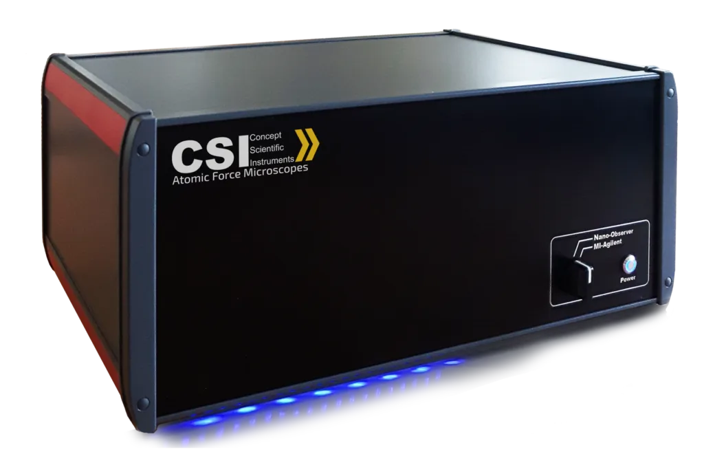
- AFM Compatibility: Nano-Observer II
- Advanced Features: Dc/Dz Measurements, Electrical Field Compensation (EFC) for MFM, Lift Mode
- Application Areas: Materials Science, Semiconductors, 2D Materials, Polymers, Life Sciences
- Lateral Resolution: Superior to standard KFM (exact value not specified)
- Sensitivity: Increased through minimized tip-sample distance and enhanced signal amplification
- Electrostatic Field Strength: 100x to 10,000x stronger than standard KFM
Note: For specific numerical values on lateral resolution, sensitivity, or other detailed parameters, please contact CSInstruments for comprehensive technical data.
Application Fields
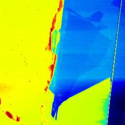
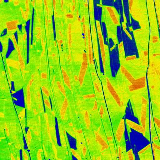
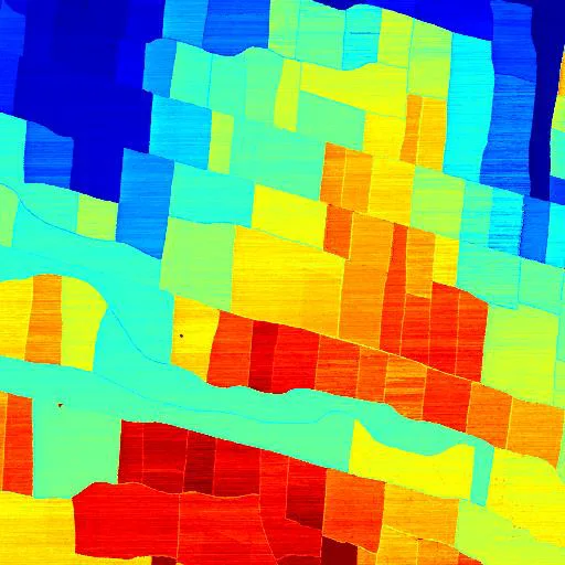
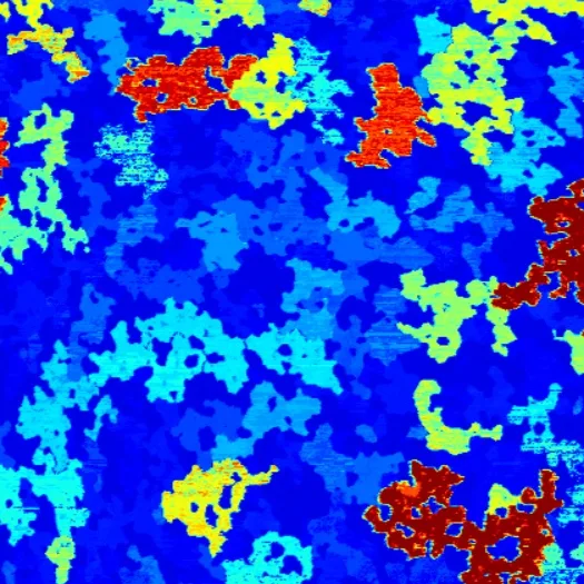
- Materials Science (Surface potential mapping, work function measurements, defect detection, thin film analysis)
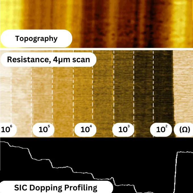
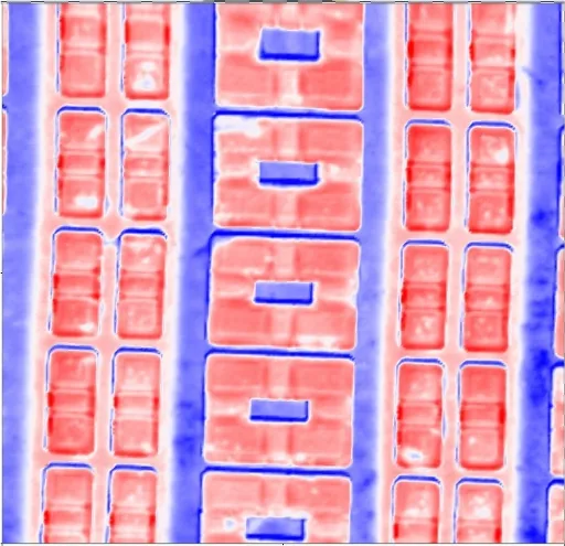
- Semiconductors (Doping profiling, device characterization, failure analysis, nanoscale electronics)
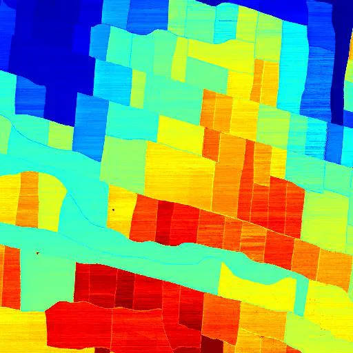
- 2D Materials (Layer identification, electronic property mapping, substrate interaction studies, defect analysis)
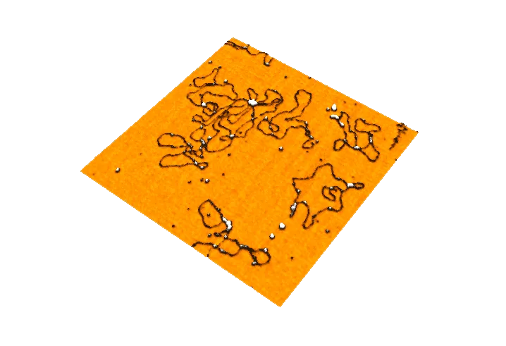
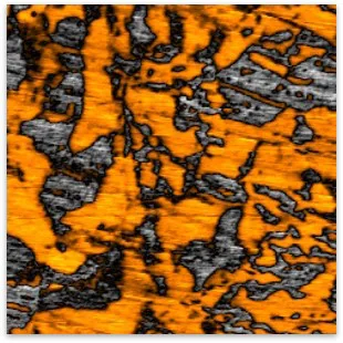
- Polymers (Charge distribution mapping, blend differentiation, aging studies, nanoscale polymer electronics)
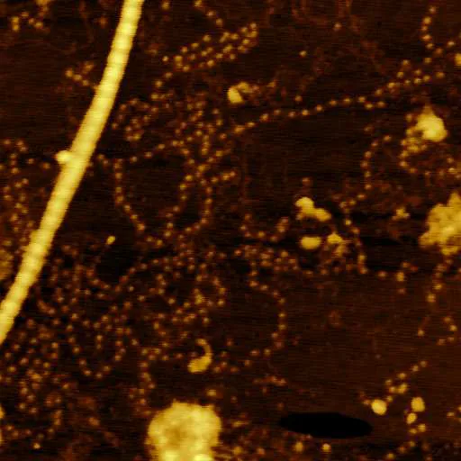
- Life Sciences (Biomaterial characterization, cell membrane charge mapping, protein/DNA charge analysis, bioelectronics)
Where it is used
Application fields for HD-KFM™ III
Combine and upgrade
Works with — and runs on
Product note
HD-KFM™ III product note
Principle, key specifications and application examples in one technical document. We send it to you by e-mail.
FAQ
Frequently Asked Questions
What is HD-KFM III?
HD-KFM III (High Definition Kelvin Force Microscopy III) is an advanced single-pass Kelvin Probe Force Microscopy module developed by CSInstruments for the Nano-Observer II AFM. It simultaneously measures surface topography and surface potential in a single scan pass using bimodal dual-frequency excitation, with a tip-sample distance of 0.1–0.5 nm — achieving electrostatic field sensitivity 100 to 10,000 times greater than standard KFM.
What is the difference between single-pass KFM and dual-pass KFM?
In dual-pass (lift mode) KFM, the AFM tip makes two separate scans: the first records topography, and the second is lifted 10–100 nm above the surface to measure surface potential. Single-pass KFM, as implemented in HD-KFM III, acquires both topography and surface potential simultaneously in one scan. This eliminates lift-height artifacts, operates at 0.1–0.5 nm tip-sample distance, and achieves significantly higher sensitivity and lateral resolution.
How does HD-KFM III achieve higher sensitivity than standard KPFM?
HD-KFM III uses bimodal excitation: the first flexural eigenmode of the cantilever is mechanically driven for topography, while the second flexural eigenmode is electrically excited for surface potential measurement. The VAC bias is automatically tuned to the second eigenmode resonance, amplifying the signal by the Q factor of that mode — often 100x or more. The close tip-sample proximity (0.1–0.5 nm vs. 10–100 nm for standard KFM) further increases electrostatic field strength by a factor of 100 to 10,000.
What materials can be characterized with HD-KFM III?
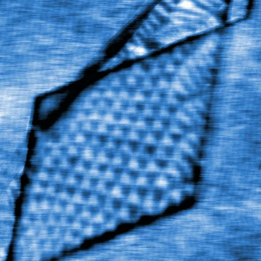
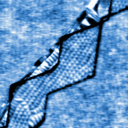
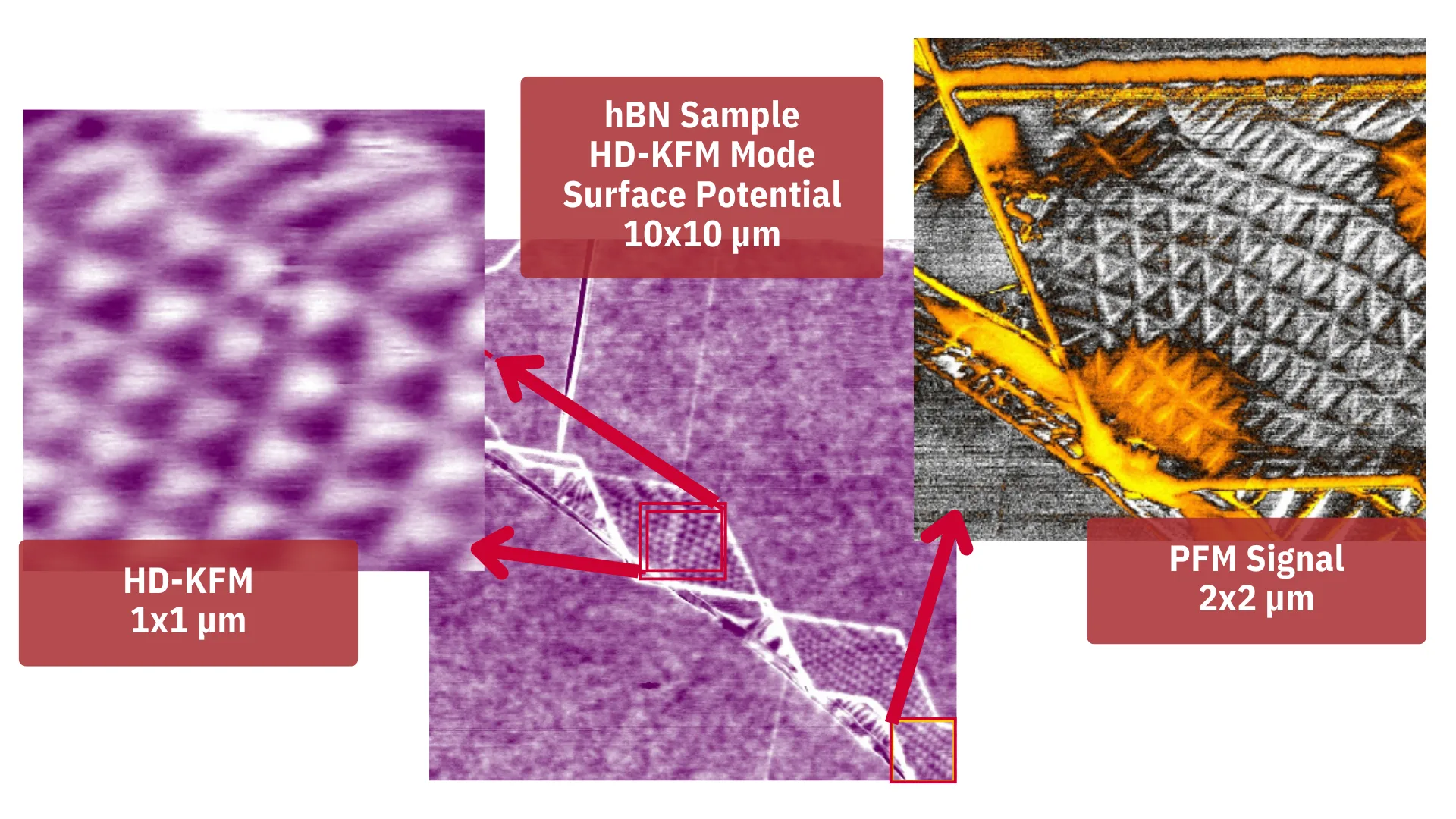
HD-KFM III is applicable to a broad range of materials: 2D materials (graphene, hBN, MoS2) for layer thickness identification and moiré pattern mapping; semiconductors for work function mapping, doping profiling, and SRAM device characterization; perovskite and organic photovoltaic materials for surface potential mapping; polymers for charge distribution; and biological samples for cell membrane charge analysis. It is also capable of simultaneous MFM and HD-KFM measurements on magnetic materials.
What AFM system is HD-KFM III compatible with?
HD-KFM III is exclusively designed for the Nano-Observer II AFM by CSInstruments. The Galaxy Dual Controller also enables HD-KFM capabilities on legacy AFM platforms including Bruker MultiMode, 5100, and 5500 systems.
Can HD-KFM III be used for perovskite solar cell research?
Yes. HD-KFM III is well-suited for perovskite solar cell characterization. It enables high-resolution surface potential mapping of perovskite thin films, grain boundary analysis, and work function measurements — all critical for understanding charge transport and photovoltaic efficiency. The single-pass mode avoids topography crosstalk that can affect standard lift-mode KFM measurements on these rough surfaces.
What is dC/dZ measurement in HD-KFM III?
dC/dZ measures the gradient of capacitance with respect to tip-sample distance. In HD-KFM III, this capability enables nanoscale mapping of local dielectric properties and thin film characterization. It is particularly useful for identifying dielectric constant variations in composite materials and insulating layers.
What is EFC (Electrical Field Compensation) in HD-KFM III?
EFC (Electrical Field Compensation) is a feature in HD-KFM III that nullifies the electrostatic interaction between the AFM tip and sample during simultaneous MFM (Magnetic Force Microscopy) measurements. This allows researchers to obtain pure magnetic contrast without electrostatic artifacts — essential for accurate characterization of magnetic nanostructures and spintronic materials.
Questions about HD-KFM™?
Ask the application scientists behind our AFMs and modes — about your samples, probes, set-up or which mode fits your measurement. We answer every message personally.